0

Driver circuit

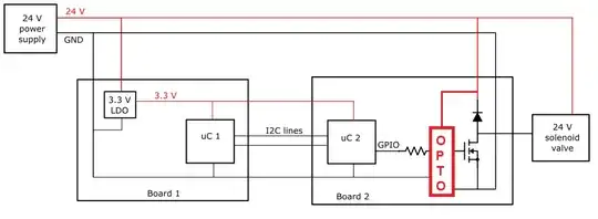
These two boards are supplied from a 24 V power supply like in the picture shown. I didn't design any of them. The first board cannot be modified at all, the second board can be modified completely. The two microcontrollers communicate using I2C through a 4-wire ribbon cable (3.3 V, SDL, SCL and GND). This communications cable is 5 cm long.

I imagine that the reason the ground of the valve driver is taken from the power supply in the second board is to keep this loop small and separated from the microcontroller ground, even if electrically it's the same point. However, I can't see if the way this is connected could be an issue or if it could be improved. The output pin toggles once a minute, but there's the option to connect a proportional valve that needs a 1 kHz PWM output from the GPIO to operate.

Marcos
  • 73
  • 6

2 Answers2

3

Could the grounding of this circuit cause any issues or be improved?

I'd be happy if it were designed like this because of the tortuous path the ground return takes: -

enter image description here

This then isolates any potential problems in driving the MOSFET effectively. The opto type I would choose would be something like an FOD8343 (although this is very high-spec having a 5 kV isolation barrier). So look for an equivalent device that has at least 1500 volts galvanic isolation capabilities and low coupling capacitance. Maybe the TLP3122.

Double-check that the rise and fall times in the opto you choose are OK for your PWM needs (hint: the FOD8343 is really quick so no problem with that even at 100 kHz).

Also double-check that your MOSFET can work with a 24 volt drive on the gate - if it can't then use a regulator to drop the local 24 volts to something like 12 volts to power the opto.

Andy aka
  • 456,226
  • 28
  • 367
  • 807
  • 1
    thanks a lot for your detailed response, I really appreciate it. The optocoupler solves the problem for the ground return path. – Marcos Feb 25 '22 at 18:00
1

Of course there can be problems, but it depends on wire lengths, wire resistance, solenoid current etc.

The FET Vgs is what controls the FET. The gate return path is source so it has a long way back via wiring and board 1 to board2 MCU. If there are large currents or fast changing currents and volages there is a possibility for problems due to large loop area.

Justme
  • 147,557
  • 4
  • 113
  • 291