5

enter image description here

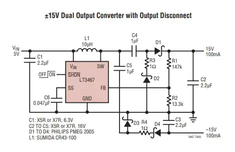
This schematic is from the LT3467 datasheet. I'm hoping someone can help me understand the purpose of the 1 ohm R3 and R4 resistors.

My concern is that they'd need to have very high power ratings as it seems there would be a ton of current running through them which would require them to be pretty large. Although in reality I don't believe that's the case, otherwise this circuit wouldn't be very practical.

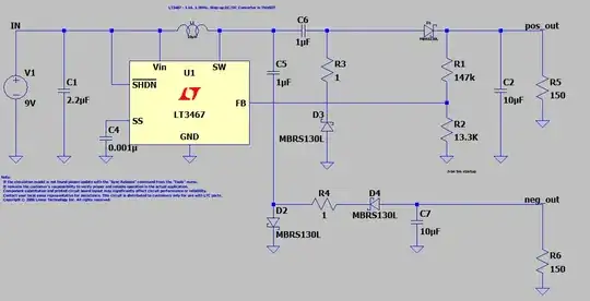
I did run a simulation in LTspice and looked at the voltage at the R3 node and the current through it. Here's the schematic and simulation output. The voltage and current are switching at the switch frequency of the device, which is 1.3MHz. The switch current swings about 820mA (maybe using incorrect terminology here?) so it seems to me the 1 Ohm resistor would need to dissipate nearly 10 watts! (15V x 640mA = 9.6W.) I feel like I'm not thinking about this correctly.
enter image description here

enter image description here

JRE
  • 71,321
  • 10
  • 107
  • 188
birdman
  • 53
  • 4
  • 2
    Have you tried zooming in on those plots to see what the waveform actually looks like? Yes, the peak current might be high, but if the duty cycle is very low, then the power dissipation will be low, too. A 1 uF capacitor can only store so much energy at 15 V. – Dave Tweed Jan 21 '22 at 15:51
  • 1
    You can view power dissipation for a component in LTSpice, in Windows you hold the ALT key while right clicking the component. You can also hold CTRL and click the trace name at the top of the waverform to see the average value. If you're using something other than Windows you'll have to find the equivalent keys to do this. – GodJihyo Jan 21 '22 at 16:21
  • 640mA through a 1 ohm resistor implies 640mV, not 15V. So, less than 1W, not 10W. –  Jan 21 '22 at 16:44
  • The peak dissipation is I^2*R, and the average will be well below that. – Spehro Pefhany Jan 21 '22 at 17:18

1 Answers1

3

Assuming the steady state RMS charge current is the same as the DC rated current of 100 mA = 0.1A .
\$P_d=I^2R= 0.1^2[\text{A}] \times 1 [\Omega]= 10\text{ mW}\$ for the resistor in question.

This split supply regulator boosts 5 V to +15 for a 10 V boost and +5 to -15 V for a 20 V boost. The Schottky diodes are all the same and rated for 20 V and the energy transfer must be greater, thus the series R must be a thermal power sharing during the power-on transient..

The biggest power load is during startup. Your results indicate the current but not the duty factor of the pulses and thus the average power is less.

I(R3) peaks at almost 5 A or 25 W for a number of switching cycles. But the tail of this envelope of peaks ends before 0.5 ms, which is much shorter (< x %) than the rated single pulse max of 2.5 A. So this adds some thermal surge sharing with the Schottky diodes which are also rated here for only -20 V. These can be prone to thermal runaway when hot as the leakage current rises sharply.

Null
  • 7,603
  • 17
  • 36
  • 48
Tony Stewart EE75
  • 1
  • 3
  • 54
  • 185