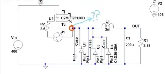
The designer was too lazy to figure out the appropriate level shifter with bootstrap.
Ok, to be more charitable, they only wanted to see how the SiC device behaved by itself, so they control gate-source bias directly. As it's an n-FET, the gate has to be driven higher than source to turn it on, but not too high such that it will cause the gate to break down. As the source is swinging up and down with the action of the switch and catch diode, that takes some work.
There are companion gate driver ICs that help solve this problem and allow you to fully realize the benefits of using SiC, notably, its faster switching time that allows higher stepping ratios. More here: https://www.powerelectronicsnews.com/gate-driver-circuit-optimization-for-sic-power-devices%EF%BB%BF/
I discuss bootstrapping here: Buck Converter Simulation in OrCAD Capture Lite
