(EDIT: After looking at your question again, I have realized that you probably know all or most of this, and that you just need to understand the circuit in question. I have addressed that towards the end of this answer (scroll down), but didn't want to remove other explanations because they might benefit others with more basic questions and because I have invested so much time and energy writing it.)
All that you have to remember about dropout voltage is that it is the voltage loss across the pass element. In a linear regulator such as LM7805 with a bipolar, NPN, pass transistor, it is about 2V. Lower voltage loss or dropout voltage is achieved using a PNP pass transistor in a positive linear voltage regulator. Almost no voltage drop is achieved with a MOSFET as a pass element at low current, because it acts like a low resistance channel.
A picture is worth a thousand words, so I will illustrate.
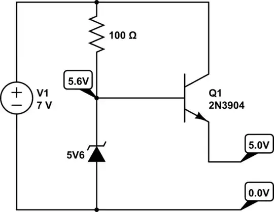
simulate this circuit – Schematic created using CircuitLab
As you probably know, whatever the voltage you want to get at the emitter (the output of the regulator), you need to provide the voltage that is at least a Vbe drop or about 0.6-0.7V above it in order to make the transistor turn on and conduct. Add to that the voltage drop across the resistor feeding the zener diode and the transistor base, and the input needs to be that much higher than the potential at the base.
THIS is what gives us the minimum voltage drop across the collector-emitter of the output transistor, even though most transistors have a much lower Vce drop when saturated or turned on. You simply can't turn the transistor on with the voltage lower than the emitter potential PLUS the Vbe drop AND the resistor drop in this case. Lowering the input voltage any further will also lower the output voltage, meaning the regulator is not keeping the set voltage at the output or regulating anymore.
Add another transistor to the output transistor to form a Darlington pair, and you increase the minimum input voltage requirement by another Vbe drop, or 0.6-0.7V:
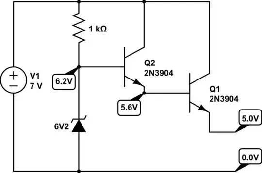
simulate this circuit
You also probably know this arrangement is done to reduce the "quiescent" current which goes to waste but is necessary for feeding the zener diode. The downside is that this also requires a higher minimum input voltage equal to 2 Vbe drops plus the resistor voltage drop, easily meaning at least 1.5V "dropout" voltage.
Which brings us to LDO or Low DropOut voltage regulators.
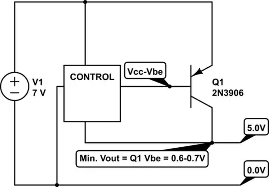
Instead of using the emitter of an NPN transistor as an output in a positive voltage regulator which needs higher input voltage to overcome the Vbe drops, a PNP transistor with its collector as an output node is used to eliminate this drop on the positive rail.
simulate this circuit
I have simply placed a box because the control circuitry for this type of regulator is a little more complex and harder to understand.
The main points about this type are:
- No need to overcome the Vbe drop on the positive side, however >
- this moves the Vbe drop to the negative rail; where the NPN type output can go down to zero volts, this one can't go below the Vbe of the Q1
- The positive rail only needs to overcome the pass transistor Vce saturation voltage which is smaller than the Vbe and can be as low as 0.1V. This is the famed LDO dropout voltage.
- The base current in this type of regulator is wasted, or taken away from the output current, while in the NPN type it was added to the output, so the quiescent or self-consumption current is usually higher for LDO regulators.
Finally, if a MOSFET is used as a pass transistor, the dropout voltage can be almost zero at lower currents, and usually the lowest of all, since MOSFET does not have Vds saturation voltage rating, but a RdsON rating, meaning its saturation resistance is specified instead of a voltage drop.
The problem with MOSFET is that it needs significantly higher gate-source voltage to turn or keep it on (2-5V), so your control circuitry has to account for that.
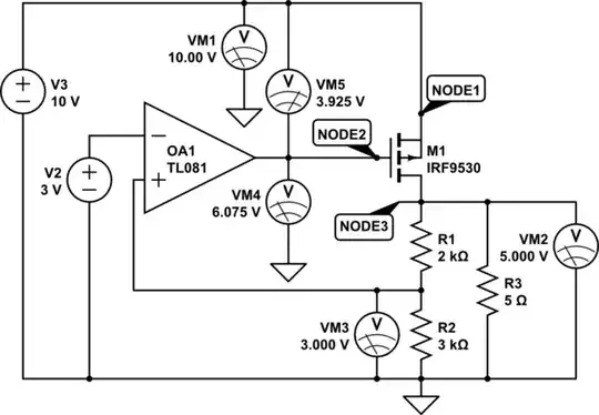
In your case:
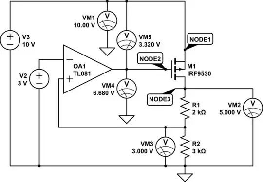
simulate this circuit
What you can see is that the VGS voltage needs to be at least at the Gate-Source threshold voltage or VGS(th) or above in order for the MOSFET to start conducting and the regulator to function as intended.
The additional requirement is that the input voltage or MOSFET source leg potential needs to be above the output voltage by the amount of voltage drop across the MOSFET drain-source channel.
For the transistor in my schematic, the threshold voltage is 3.32V, and the minimum channel resistance in saturation is around 0.3 ohms.
This means that even if your output voltage is at 0 volts, your supply voltage needs to be at least 3.32V just to turn the MOSFET on, and 4.32V if output is 1V.
If you experiment with the supply voltage value, you will notice that it becomes unpredictable once you go below 5.001V because that is the output voltage of 5.0000V plus the voltage drop at 1mA (0.3 ohms x 1mA = 0.0003V or 0.3mV).
What happens is that because the input voltage is lower than the output voltage, the op-amp raises the VGS significantly higher than the threshold voltage in order to open the MOSFET more and keep the output at the required level, which eventually leads to the supply and VGS (and almost the output as well) voltages being equal and bringing the output voltage out of the regulation.
Now, in your case, if we add a 1A load at the output, the voltage drop across the drain-source channel will be about 0.3V, which means you need at least 5.3V input power supply.
Also, at increased load currents, the needed VGS(th) increases to open the drain-source channel more.
Below is the same circuit with an added load resistor. As you're editing its value, the voltmeters in the circuit instantly reflect the change even while the resistor value editing window is open and you have not saved it.
simulate this circuit
P.S.: Your formulas and symbols are a little unclear to me. I admit I'm not that good with math, but I think that you're not that good with it either, and that you're trying to comprehend a concept through mathematical formulas before comprehending it visually and experimentally, which is the opposite of how people learn and understand in general.
Always try to visualize before going into mathematical formulas and equations because they only get you even more confused before you get to understand a concept.
