About designing AND gate using N-type mosfets: first image is used everywhere. However, it uses an additional inverter part. Is it not possible to design the circuit like below (second image)? If not, what is the reason for that?
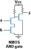
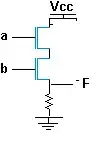
About designing AND gate using N-type mosfets: first image is used everywhere. However, it uses an additional inverter part. Is it not possible to design the circuit like below (second image)? If not, what is the reason for that?
It would sort-of work, however the logic levels on the output would be so poor ('1' wouldn't be high enough) that the next stage wouldn't see good logic levels...
Depending on the MOSFETs used (specifically their threshold voltage), this problem might be solvable, but in practice the standard solution is much easier despite the extra stage.
This is why earlier logic families used NAND gates instead of AND gates - they eliminated the inverter stage and inverted the logic levels for the second stage.
Since the second stage was usually an OR stage (implementing (a and b) or (c and d)), and 'OR' with inverted logic is just 'AND', this meant that "AND-OR logic" was implemented with two levels of NAND gates, and the outputs were right way up again!
This method does work, provided the resistance is high enough to minimize current and allow for a clear high.
There are problems however:
Vgs is the primary control for a MOSFET used as a switch. The current through the resistor can cause the source voltage to rise enough to where a high logic value on the bottom MOSFET gate does not switch the MOSFET fully, as Vgs is smaller, making the MOSFET more likely to enter its active region, thereby wasting more power.
In my opinion, the big issue is fanout. In the inverter form, the logic high has almost no current lost to the transistor, meaning all current essentially comes from the voltage source. This equals current that can drive other gates. In your form, the logic high has current split through the resistor and the output. So current demands for yours are VDD/Rload + VDD/R, where as the other way has VDD/(R + Rload).
Those circuits are Resistor Transistor Logic. It is obsolete and has been replaced by TTL and CMOS. Realistically CMOS is all you see for a decade or two.
The drive capability of an NFET is limited by the voltage difference between its gate and whichever other terminal is higher; in many cases, it will fall off to practically nothing as the voltage difference falls below about ~1.5 volts. It's thus rather difficult for an NMOS chip which does not have a bias source above 5 volts to pull up anything above about 3.5 volts, and a transistor whose gate is at 3.5 volts will have a hard time pulling its output above about 2 volts. There are times when it is useful to have a transistor pull something "high", but transistors cannot do a good job of it unless their gate is a very solid high and their output isn't going to have to drive much. By contrast, with inverting logic, everything can output a solid low, and nothing needs an especially solid high.