I'm new to this concept and parts of it are a little confusing. I understood the part when a 5V signal is applied as input, a channel is formed in the NMOS device, as the positive voltage attracts electrons, thus output is connected to the ground via the NMOS and hence 0 output. But when 0 volts is applies to the gates of both the devices how does the PMOS conduct for the output to be high? Since both are enhancement mode devices a channel does not exist beforehand and is brought about by introduction of a gate voltage. When 0 gate voltage is applied how does a conducting path get formed in the PMOS for the output to connect to VDD?
Asked
Active
Viewed 1,615 times
2
-
Need a schematic... – Matt Young Nov 22 '12 at 05:47
-
I cant add a picture because I just joined and don't have enough rep yet but it is the basic cmos inverter. – Arun Suryanarayanan Nov 22 '12 at 06:33
-
A PMOS device turns on when there is a voltage between the source and the gate that exceeds the threshold voltage. The source is at +VDD and the gate at 0V in the on state. – pjc50 Nov 22 '12 at 09:30
-
If you added a link, someone could have edited it for you. – Matt Young Nov 22 '12 at 16:54
2 Answers
1
Remember that the gate voltage of the PMOS device is relative to its source terminal, which is connected to the VDD supply. So, when the input to the circuit is at 0V, there is a gate bias on that device of VDD; this is what turns it on and pulls the output high.
Dave Tweed
- 172,781
- 17
- 234
- 402
0
A high voltage on the gates will cause the nMOSFET to conduct and the pMOSFET not to conduct and a low voltage on the gates causes the reverse. THe complementary arrangement with common drains and gates allows a common gate voltage with respect to ground to determine which one conduct. What happens in between is also very interesting and not shown is a small bulk resistor on the drain of the n type. (eg 10R)
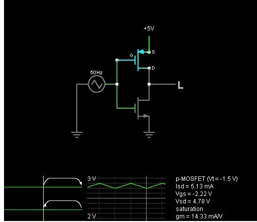
Let me post a schematic for you with a simulator.
Each single stage CMOS inverter is designed to have a voltage gain of 10, a buffered one is 3 stages so the gain is 1000. I took the liberty of showing the VI curve of each device and the input being a sine wave 500mV biased at Vcc/2. The simulator is here.
THe MOSFETS have equal and opposite polarity thresholds of 1.5V and conduct 10mA during the accelerated transition period.
Tony Stewart EE75
- 1
- 3
- 54
- 185
-
So if this has to work as a NOT gate, logic 0 should correspond to a voltage less than -1.5V and logic 1 greater than 1.5V? – Arun Suryanarayanan Nov 22 '12 at 07:28
-