Are there any low-cost and accurate ways to measure small dimensions on a physical PCB? Physical is critical here, since it's easy to measure dimensions in a CAD tool. However, actual dimensions will diverge somewhat from the design dimensions due to manufacturer tolerances. In particular, I'm interested to know how closely the width of my \$50\,\Omega\$ traces are to the design specs.
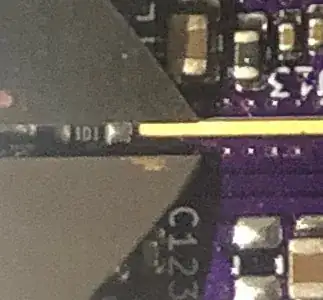
Here's what I've tried: I've taken a picture of a PCB trace adjacent to a set of calipers measuring 1.01mm (idea taken from here). I can then measure the pixels in GIMP (though I'm sure other image editors can do this too). The ratio of the trace to caliper pixel widths times the caliper width gives me the trace width. However, the image is a bit blurry. I think the reason for this is that my iPhone camera cannot support a very short focal length and does not have an optical zoom. I did rest the camera on a stable surface so it wouldn't move. I'm not a photographer, so if there's a way to get better results please let me know. Moreover, the result is a bit far off what I'd expect. I designed these trace widths to be 0.38mm, but am getting about 0.43mm (bear in mind the blurriness makes it difficult to be accurate here). Here's the image. The PCB is manufactured by oshpark 4-layer.
Any thoughts on this process, or better processes available? I know there are dedicated tools that will do this (e.g. some dinolight microscopes will measure distances), but from what I've seen, those are all expensive solutions.

