You'll want to research "high side" and "low side" transistor switch circuits.
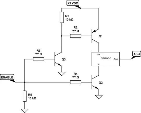
Transistor Q1 should not be an NPN type BJT (nor an N-type MOSFET) because it cannot turn on completely (it cannot be driven into saturation) due to the positive voltage at the transistor's emitter pin. In a circuit like yours, the "high side" transistor switch should be a PNP type BJT (or a P-type MOSFET) with the BJT's emitter (MOSFET's source) connected directly to the +5V power supply and the BJT's collector (MOSFET's drain) connected to the sensor's V+ pin. You'll need to add a current-limiting resistor to the PNP transistor's base to limit the base current to a safe level (see also my comments below).
If you change Q1 to be a PNP type BJT, you'll discover you cannot turn off both Q1 and Q2 with a single digital logic "ENABLE" signal. If ENABLE is logic LOW, then Q1 will be ON and Q2 will be OFF. Likewise, if ENABLE is logic HIGH, then Q1 will be OFF and Q2 will be ON. You can solve this problem by adding a third transistor Q3 (an NPN or an N-type MOSFET) whose job is to invert the ENABLE signal at Q3's base as shown in Figure 1 below.
When the ENABLE output is in its HIGH-Z state (i.e., when ENABLE is not actively driven logic HIGH or logic LOW), pull-down resistor R5 weakly pulls the voltage on the ENABLE node down to approximately 0 VDC (logic LOW). See the next bullet.
When ENABLE is logic LOW, transistors Q2 and Q3 are driven into CUTOFF (they are off). Pull-up resistor R1 weakly pulls the voltage at Q1's base up to about +5 VDC, driving Q1 into CUTOFF.
When ENABLE is actively driven logic HIGH, transistors Q2 and Q3 are ideally driven into SATURATION (they are fully on). The voltage at Q3's collector is close to 0 VDC, which causes current to flow through Q1's emitter-base diode, through resistor R2, and through Q3 to ground, which ideally drives Q1 into saturation (it is fully on).
The resistance values of base resistors R2, R3, and R4 must be chosen so that when the ENABLE signal is logic HIGH, the base currents in transistors Q1, Q3, and Q2 (respectively) are sufficient to drive these three transistors into SATURATION (fully on). Calculating values for these base resistors is a straightforward process: see [1] and [2] in the REFERENCES section below. Note that the digital input/output (DIO) pin that actively drives the ENABLE signal must be capable of sourcing all of the current (the combined current) for these three current paths: the current through resistor R5, plus Q2's base current, plus Q3's base current, i.e.,
$$
I_{DIO(ENABLE)} = I_{R5} + I_{Q2B} + I_{Q3B}
$$
simulate this circuit – Schematic created using CircuitLab
Figure 1.
:: IMPORTANT ::
The voltage at the sensor's V- power pin will not be ground (0 V); it will be some positive voltage that is determined by Q2's collector-emitter voltage drop. Consequently, the sensor's output voltage Aout will be relative to Q2's collector voltage; it will not be relative to ground. Likewise, the voltage at the sensor's V+ power pin will not be +5 VDC, and therefore the sensor's output voltage Aout might be different than it otherwise would be if the sensor's V+ pin were connected directly to +5 VDC.
REFERENCES
[1] https://electronics.stackexchange.com/a/485252/79842
[2] https://electronics.stackexchange.com/a/488355/79842


Note that when you use the CircuitLab button on the editor toolbar and "Save and Insert" on the editor an editable schematic is saved in your post. That makes it easy for us to copy and edit in our answers. You don't need a CircuitLab account, no screengrabs, no image uploads, no background grid.
– Transistor Nov 05 '19 at 15:16