Segue into a design
If you find the following an unwanted digression about BJTs, feel free to skip to the design section below. But for some, this may help a little to set the tone of what follows in the design section.
I want to start out by stating two things:
- Design constraints matter a great deal in how one goes about arranging a design process to follow.
- While design constraints matter, they do NOT determine a design process. Creativity, awareness, and toying with ideas can have an important role to also play and can even substantially transform the design process on occasion.
A conclusion from the above (if you are at a point where you can accept what I just wrote in the light it is meant) is that your question is, in some very fundamental ways, misguided. And it is still just as misguided, even if the question is greatly improved by providing a host of reasonable design constraints (which are mostly lacking in your question, right now.)
So let's start out with some ideas that are essential to have in mind when designing a discrete single-stage BJT amplifier. (There is a family of such topologies which will mostly share what follows.) These are just the ones associated with BJTs themselves that may place inherent constraints on a circuit design and, by implication, the process used in discrete designs (the world within IC design will have very different considerations than what I write about here):
While a BJT's \$\beta\$ will be remarkably constant over a span of from three to five orders of magnitude of collector current, that's only true when talking about one specific BJT operating at one exact temperature. (And even then, it may drift over time.) So, if you are designing for the purpose of just making one prototype circuit to solve a one-time problem and you know that the temperature won't vary much (such as a device you will wear taped to your body), feel free to design a circuit that depends upon a measured \$\beta\$. But in all other cases, such as when more than one will be built or where the temperature might range over dozens of degrees Celsius, then you need to design a circuit which is thermally stable with respect to changes in temperature and device. As a general rule, for general-purpose small-signal BJT devices I usually seek something that is stable with \$100 \le \beta \le 300\$. For any other purpose, I know I have to study the device family specifications to come up with a better estimate of the range.
The active-mode \$V_\text{BE}\$ depends on the collector current, the emission co-efficient, the operating temperature of the device, the device family, and the particular device you picked out. For general-purpose small-signal BJT devices drawn from the same BJT device type operating at the same collector current and temperature, I expect the differences between any two of them as: \$\mid\, V_{\text{BE}_1}-V_{\text{BE}_1}\mid\:\le 30\:\text{mV}\$. But temperature impacts this: \$1.8 \frac{\text{mV}}{^\circ\text{C}} \le \frac{\text{d}}{\text{d}\, T}\, V_\text{BE} \le 2.4 \frac{\text{mV}}{^\circ\text{C}}\$ over "normal" temperature ranges (and this rate is, itself, temperature-dependent even for a single device -- so you can't treat it as a constant even for a "one-off" project.) It's best to use the larger end, namely \$2.4 \frac{\text{mV}}{^\circ\text{C}}\$, if you want a "constant" to use for estimating the variation you have to tolerate. This will likely cover variations between devices as well as over temperature.
For DC operating point stability with respect to temperature and part variations and so on, given an emitter-degenerated topology like yours, it is at least 10 times more important to worry about variations in \$V_\text{BE}\$ than it is to worry about variations in \$\beta\$. (I can prove this mathematically, but you can take it as given or else read here for a part of why.) Both will have an impact. But if you focus on only one of them, focus on making sure your circuit's DC operating point is sufficiently stable against variations in \$V_\text{BE}\$ over temperature, time, and device. In fact, the design choices with respect to the emitter are mostly about this consideration. Some desired voltage gain almost doesn't even factor into it, unless other constraints force the issue to the surface.
For AC (small-signal) voltage gain purposes, \$r_e\$ is proportional to absolute temperature and inversely proportional to the collector current. Changes in \$r_e\$ impact \$A_v\$ and therefore impact signal distortion. Designing to minimize the impact of temperature on distortion is something you can attempt to address during the design process. But once a circuit has reached thermal stability after being powered up, unless the operating temperature changes a lot as the signal varies, it can be neglected. What does matter a lot, though, is the collector current itself is almost always highly impacted by the signal input. If lower signal distortion is important to a design, then the inevitable signal-dependent variations of \$A_v\$, due to signal-dependent variations of \$r_e\$, need to be addressed satisfactorily in the design process.
It turns out that the voltage supply rail (and its characteristics that you can specify or uncover) has a fairly large impact on which of the above considerations dominate a design process. If you are constrained by \$V_\text{CC}=3.3\:\text{V}\$, for example, you really don't have a lot of room for easy choices. The design process will be more about deciding "how bad" the situation is and how much of each problem you can balance out and accept. But with \$V_\text{CC}=20\:\text{V}\$? A lot of that goes away and you can readily deal with device and temperature variations (basically, just "spend" some of the available \$V_\text{CC}\$ to address them and then stop worrying about them.)
(In the above, I've avoided discussing high frequency oscillations, voltage gain variations over frequency, and other factors due to "unseen" parasitics. For most of my purposes now, I'm caring about discussing DC aspects and I'm assuming, if pressed, only those frequencies that are easily achieved by such a circuit; leaving other difficulties for another time.)
There are other considerations, of course, which reach beyond the BJT device's inherent "flaws." These include the signal source's characteristics and what the circuit will also be driving. (The circuit can actively pull down on the load, but can only passively pull up on the load, as just one thing to keep in mind when thinking about what the circuit is supposed to "drive.") The power supply itself also matters. For example, is it to be a \$9\:\text{V}\$ battery which may have \$2\:\Omega\$ of source impedance (or more) and widely varies in voltage over its useful life? Does the power supply have substantial "ripple" or is it "dead flat" and stable? And so on.
It's important to collect and consider as much hard information as you possibly can, while at the same time taking note of what you don't and cannot control. (Luckily, a circuit like this isn't so often used as a "first stage" section and almost never is used as a "last stage" section. So it usually sits between two other sections that are under your control. (A saving grace, so to speak.)
(I almost never use this topology without the added support of bootstrapping the base divider from the emitter node. It costs one added resistor and capacitor and provides huge benefits with very little down-side. So, just as an FYI to you, I consider this more of a "teaching how to design a DC stable BJT stage" than anything I might use in practice.)
Finally, some of the difficulties mentioned above regarding a single-stage design like yours can be addressed through what's collectively called "global NFB." In general terms, this just means surrounding a circuit with other circuit elements which can observe and then rectify issues with the current stage you are working to design. Global NFB can be DC in nature if it observes something and then adjusts and/or acts to stabilize the DC operating point of your amplifier stage. It can be AC in nature if it observes and then adjusts the desired \$A_v\$ of the over-all system (vs frequency.) Professionals will use every trick they know in balancing out local NFB choices with global NFB choices to create a final design (consistent with the time they have available of course.) Hobbyists can make differing calculations, though.
I hope the above discussion convinces you that there isn't a single one size fits all design process.
Design steps for a \$20\:\text{V}\$ rail with unknown \$A_v\$, unknown source impedance, unknown load, and pretty much everything else unknown except that there is a BJT and four resistors
Note: Well, the one good thing here is that \$V_\text{CC}\$ is actually given and that it is in the ball-park of \$V_\text{CC}=20\:\text{V}\$, which means we have a lot of voltage headroom to work with. However, since I've no idea how solid that rail is or if it might have a fair bit of ripple, perhaps the first thing I might consider doing is to "filter it." (Create a known source impedance with an added resistor and include an added capacitor as the new "rail" I rely upon. This would be a simple RC filter, in effect, that I'd design into the over-all design.) In this case, all I'd be doing is complicate your circuit. So I'll leave that bit out in what follows and head more in the direction of what I think you really want. (It won't take long because there's not much to work with, yet.)
Here are my thoughts as they arrive:
\$V_\text{CC}=20\:\text{V}\$, which is a lot, so I can afford throwing away/reserving some to deal with temperature and device variations on \$V_\text{BE}\$. Let's say I want to accommodate a span of \$50^\circ\,\text{C}\$ and individual BJT in-family variations, then I want to cope with \$50^\circ\,\text{C}\cdot 2.4 \frac{\text{mV}}{^\circ\text{C}}+30\:\text{mV}=150\:\text{mV}\$ of \$V_\text{BE}\$ span. Dividing the span in half, I estimate \$\Delta V_\text{BE}=\pm 75\:\text{mV}\$ around my design choice of \$V_\text{BE}\$ for operating conditions and device vagaries. It turns out (I can show the math, if needed) that:$$V_{\text{E}_\text{Q}}\ge\frac{\Delta V_\text{BE}}{\%\,I_{\text{C}_\text{Q}}}$$ where \$\%\,I_{\text{C}_\text{Q}}\$ is the percent variation of \$I_{\text{C}_\text{Q}}\$ I'm willing to tolerate and \$\Delta V_\text{BE}\$ is the maximum variation above (or below, but not both) my designed \$V_\text{BE}\$. Suppose I wanted to tolerate only \$\%\,I_{\text{C}_\text{Q}}=1\,\%\$. Then I'd need to reserve out \$V_{\text{E}_\text{Q}}=7.5\:\text{V}\$. I know that's crazy, so I would accept more variation to get a lower quiescent value. In this case, I may decide (make a design choice) to accept \$\%\,I_{\text{C}_\text{Q}}=5\,\%\$ and therefore get \$V_{\text{E}_\text{Q}}=1.5\:\text{V}\$.
(The choice you show on your schematic allows \$\%\,I_{\text{C}_\text{Q}}=7.5\,\%\$ variation. That's an arguable position to take.)
Note that the above work is only related to variations of \$I_{\text{C}_\text{Q}}\$ with respect to part and temperature variations. This has nothing to do with the normal AC variation of \$I_\text{C}\$ when a signal is applied. That's a different consideration, entirely. (Important -- but separate.)
At this point, I need to think about a different relationship: \$V_{\text{C}_\text{Q}}=V_\text{CC}-A_v\left(V_{\text{E}_\text{Q}}+V_T\right)\$. I can tentatively ignore \$V_T\$ (the thermal voltage) since it is relatively small. Then \$A_v=\frac{V_\text{CC}-V_{\text{C}_\text{Q}}}{V_{\text{E}_\text{Q}}+V_T}\approx \frac{V_\text{CC}-V_{\text{C}_\text{Q}}}{V_{\text{E}_\text{Q}}} \$. Since you haven't specified \$A_v\$ for this circuit, I can't compute \$V_{\text{C}_\text{Q}}\$. But at least you can see that larger values will require a lower quiescent operating point for the collector's voltage.
Step 2 brushes up against a different issue. With your \$V_\text{CC}\$ being "adequate for most uses," I can also afford to throw away some of it to deal with \$\beta\$ variations vs \$V_\text{CE}\$ and also the Early Effect. Here, a larger value for \$V_{\text{CE}_\text{MIN}}\$ is often better. But, of course, reserving it tends to mean lower available \$A_v\$. So, this is another trade-off item I'd want to address if you'd supplied more information.
I still haven't yet chosen \$I_{\text{C}_\text{Q}}\$. (Note: your circuit doesn't include a bypass capacitor in the passive emitter leg circuit to allow the quiescent DC operating point to be set separately from the desired \$A_v\$, at AC.) It's not really possible to decide this until after I know what I'm driving with the circuit (and what's driving the circuit.) So, once again, this becomes yet another issue that's deferred until more detail is supplied.
I could assume that it is being driven by a source with zero source impedance and that it is driving a load with infinite impedance. In such an idealized case, I'd probably just pick a BJT and then go look more closely at its datasheet for some value I could defend well. In practical circuits, a well-defended choice of \$I_{\text{C}_\text{Q}}\$ balances power supply, BJT, slew rate, input, output, gain, and bandwidth considerations.
Note: With what you write about \$V_{\text{C}_\text{Q}}=10\:\text{V}\$ and \$V_{\text{E}_\text{Q}}=1\:\text{V}\$, the voltage gain will be (with \$V_T\approx 28\:\text{mV}\$ to be conservative) less than \$A_v\approx \left(9.7 = \frac{20\:\text{V}-10\:\text{V}}{1\:\text{V} + 28\:\text{mV}}\right)\$ (ignoring input and output attenuation.)
That's about it, for now. There really isn't enough information for setting up the collector and emitter sides of this circuit, so I'd like to hold short of analyzing the base biasing pair aspect. This does get into the loading that this circuit would present to whatever is driving it and the associated attenuation of the signal before the circuit can attempt to amplify it. (And it could lead into a discussion on bootstrapping, as well.)
A Sample Design
Suppose I select this OnSemi PN2222A device and lets say I want to operate it as a stand-alone circuit that I can use for a variety of purposes. Many opamps support an output current compliance of \$15\:\text{mA}-25\:\text{mA}\$. And skimming the PN2222A's datasheet it seems as though OnSemi performs their speed tests at \$I_\text{C}=15\:\text{mA}\$, or so, and that their gain-bandwidth specification is given for \$I_\text{C}=20\:\text{mA}\$. So I've just argued myself into running this at \$I_{\text{C}_\text{Q}}=20\:\text{mA}\$. That is smack in the middle of their curves and specifications and it provides decent current compliance for something I might want driven by this circuit. So that's my call here (just to call something.)
I'm also just going to pick a number (I know it must be less than 10) for the voltage gain and call it \$A_v=5\$, so that I have something to work with.
- \$V_{\text{E}_\text{Q}}\approx 1.5\:\text{V}\$; from step 1 above, where I chose \$\%\,I_{\text{C}_\text{Q}}=5\,\%\$ for BJT/temp variances.
- \$V_{\text{C}_\text{Q}}\approx 12.4\:\text{V}\$; from step 2 above.
- \$R_\text{E}=75\:\Omega\$.
- \$R_\text{C}=390\:\Omega\$.
- \$I_{\text{B}_\text{Q}}\le 200\:\mu\text{A}\$ (the datasheet suggests \$\beta\ge 100\$ is conservative enough.)
- \$V_{\text{BE}_\text{Q}}\approx 700\:\text{mV}\$ (from figure 11 of the datasheet.)
- \$V_{\text{B}_\text{Q}}\approx 2.2\:\text{V}\$.
- \$R_1=8.5\:\text{k}\:\Omega\$. (The top resistor of the biasing pair should source more than \$10\times I_{\text{B}_\text{Q}}\$.)
- \$R_2=1.2\:\text{k}\:\Omega\$. (Accounting for worst case base drive.)
Now, the above assumes a likely worst case, in terms of the base current. So, it will probably require less than assumed above, which will raise \$V_{\text{B}_\text{Q}}\$ and run the circuit somewhat "hotter" than planned. If, for example, the base requires only half of the assumed worst case above, then there will be an additional \$100\:\mu\text{A}\$ added to \$R_2\$'s current, driving the base voltage upwards by \$\approx 120\:\text{mV}\$ and adding another \$1.6\:\text{mA}\$ to the designed \$I_{\text{C}_\text{Q}}=20\:\text{mA}\$. (It won't be quite that much of an increase, because now the base will require a little more recombination current which will act to slightly reduce the base voltage, in response. But we don't need to refine it, further.) This means the quiescent collector voltage will be about \$600\:\text{mV}\$ lower than planned. (This variance can be arbitrarily reduced by increasing the stiffness of the biasing pair, at a cost of more current consumption and decreased input impedance.)
Here's the schematic:
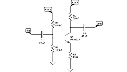
simulate this circuit – Schematic created using CircuitLab
I added a couple of capacitors. Feel free to remove them, if you prefer.
But if you plug that circuit into Spice, my bet is that you will see something remarkably close to \$A_v=5\$ (if you drive it with a low impedance source, of course.) And if you build one, it will work close to plan, as well.
Note that I chose the collector current based more about how the circuit may be used. (It was a nice coincidence that the BJT I selected also supported that choice, well.)

