0

I have a circuit where a 12V square wave signal (a Profile Ignition Pickup signal from a Ford EDIS ignition module) was fed to an MCU via a MAX232 chip. My understanding of the MAX232 is that the signal polarity is inverted and level shifted to 5V. In the original circuit design, the MAX232 was also used to convert RS232 to TTL for comms with the MCU.

I have omitted the COM port and the MAX232 from my design. I only have the PIP signal which I need to convert and want to use minimum components to do so. My thinking is that a CMOS inverter MOSFET arrangement would do this.

CMOS Inverter

Is this a valid solution?

Joe
  • 183
  • 13
  • You could consider an MC1489: essentially the receiver part of a MAX232. Or keep the max232, and leav out the capacitors (because you don't need the line driver, only the receiver). – Wouter van Ooijen Jun 16 '19 at 15:04

3 Answers3

4

Profile Ignition Pickup processing for an MCU input

You circuit will work but I'd make the following comments:

  1. It is subject to some minor shoot through (when both FETs are ON). With your circuit the problem is very minor (10's uA) at 25degC and worst case probably less than 1mA at 100degC, so you can probably ignore it.

  2. It has very poor static (ESD) capability and you are very likely to blow a FET when the input cables are disconnected. Even a simple series 1k Ohm and 100k Ohm resistor from the FET Gates to Gnd would help control this.

  3. The voltage switching point is quite low (less than 2V) for a 12V system.

  4. There is no hysteresis in the input circuit, so it may be prone to noise.

schematic

simulate this circuit – Schematic created using CircuitLab

In the schematic above I've included R2 and R3 to provide some pulse protection, but you really should have an ESD diode (20V) across R2 to provide real clamping.
The waveform would be as below:

enter image description here

A more effective circuit is shown below:

schematic

simulate this circuit

In the schematic above I've shown a TLV6001 opamp used as a comparator. This device is effective as it is designed with an inbuilt clamp to the power supply rated at 10mA.
Since the R'Pi 3V3 power supply is consuming much more than 10mA (and has significant capacitance), there is no problem in sinking current into the supply during pulse conditions. This circuit could withstand 100V on the PIP line without damage.

Note: D1 is only shown in place for the simulation, the clamp diode is actually inside the TLV6001.

The threshold points are set to 3.3V rising and 2.8V falling, so giving about 500mV of hysteresis.

The waveforms are as shown below, though I used a triangle wave for the simulator.

enter image description here

Update: Considering the need for small risetime values.
I particularly selected this device as the slew rate for the TLV6001 is 0.5V/us, which seems more than adequate for this sort of low frequency application. In a high noise electrical environment such as an automobile you don't want or need very sharp edges. For a Crankshaft sensor application the sensor frequency is just 200Hz at 6000rpm with a sensor output in the ms pulse width range. One rotation of the crank at 6krpm is 10ms or about 27us/deg. With a 10us risetime you can expect position uncertainty less than 0.3deg of rotation. Since I assume you are trying to calculate spark advance in the 10-12deg range I'd consider this more than adequate. You already have software delays which are going to far exceed this level of uncertainty.

Jack Creasey
  • 21,729
  • 2
  • 15
  • 29
  • I like the TLV6001 solution. A couple of things; the PIP signal is square wave and the MCU operates on 5V logic. I simulated your circuit with these changes and it appeared to be fine but I'm just wondering if I would need to change any resistor values to better suit 5V logic? – Joe Jun 17 '19 at 14:04
  • 1
    No changes required at all. The RPi I/O is 3V3, so you still need to connect to that pin for the TLV6001 VDD and the end of R2. All the Raspberry Pi I/O is 3.3V levels NOT 5V. DO NOT CONNECT THE TLV VDD TO 5V. Internally the R'Pi uses 5, 3.3, 1.8 and 1.2V depending on the model. The fact that PIP is a square wave makes no difference at all.....I only used a triangle in the simulator to more clearly show the threshold points. – Jack Creasey Jun 17 '19 at 14:49
  • I should stress that I'm not using a Raspberry Pi, it's actually an NXP MCU which does use 5V logic. Does the need for a 5V solution mean that the TLV is not suitable? The datasheet says the supply can be anywhere between 1.8V to 5.5V. – Joe Jun 17 '19 at 14:58
  • 1
    No, the circuit will be fine at 5V. Your threshold levels will move to 5V of course. For some reason I was fixated on R'Pi. – Jack Creasey Jun 17 '19 at 15:02
  • The voltage wont matter, just pass in what ever it is you want logic HIGH to be. – hekete Jun 17 '19 at 15:08
  • Having looked into this further, my only concern is the time between a state change occurring on the PIP signal input and the MCU logic input state change. The minimum input high on my MCU is 3.5V so I think there is about a 12uS delay between the PIP input and the MCU seeing that change. If I'm reading the MAX232 datasheet correctly, that same state change is in the order of nanoseconds? – Joe Jun 17 '19 at 18:38
  • In fact I'm looking at the MAX3180 and wondering if it's a better fit? – Joe Jun 17 '19 at 19:17
  • The slew rate for the TLV6001 is 0.5V/us. You will not see more than 10us for the 5V change and 7us for a 3.5V change. The MAX3180 will be faster, but is likely to be very much noisier with only a 1.5V threshold. Looking at images such as this: https://www.picoauto.com/library/automotive-guided-tests/edis-unit-pip-saw-signals I seriously doubt you need to chase nano second risetimes in ms signals. – Jack Creasey Jun 17 '19 at 21:16
  • I was thinking that the PIP signal is a direct translation of the crank sensor in that every 10 degrees of crank rotation (36-1 trigger wheel) you would get a pulse which would make it 3.6KHz @ 6000RPM - roughly 139uS pulse width for 50% duty. As you rightly point out, since the PIP signal occurs with every coil firing event which for a 4 cylinder engine is 200Hz @ 6000RPM - 2.5mS pulse width. – Joe Jun 18 '19 at 13:30
  • I'm still not sure why you are chasing ns level risetimes. The cabling in an auto is not set up for this. What you need is a repeatable signal not fast risetimes. You won't use a pulse from the crank sensor to trigger a coil/EHT event ….the firing point is calculated by the ECU. Reading this: http://www.megamanual.com/ms2/EDIS.htm it seems your EDIS system is expecting a VR sensor and not a Hall Effect sensor. I'm not sure what you are working with but if it's a variable reluctance pickup then your risetimes are even slower. The circuit above should still work. – Jack Creasey Jun 18 '19 at 16:05
  • Correct. I was mistaken in thinking that the rise time of this solution would be a problem but now I understand the PIP signal, I realise that it won't be. I'm making a modified version of the MegaJolt ignition control system so I will implement the TLV as per your answer and see how I go. – Joe Jun 18 '19 at 16:26
1

Your design is essentially a CMOS logic inverter: when PIP is logic HIGH, PIP_UC is logic LOW and vice versa.

The first concern is that the +5V supply could have a low impedance path to ground through Q1 and Q2 when these transistors are both conducting for a brief time as they change logic states. The +5V power supply and any circuits connected to the +5V supply must be able to tolerate this. See regions A, B, and C, and the graph of IDD vs. Vin on page 18 in this PDF.

If you perform an Internet search using the keywords "logic level converter" you'll find some simple circuits that can do what you want. The circuit that's commonly used is based upon a single NMOS transistor with two resistors (one resistor between the source pin and +5V (the lower voltage side), and the other resistor between the drain pin and +12V (the higher voltage side)), and the gate pin connected to +5V. And the circuit I'm thinking of supports bidirectional communication. (Unfortunately I cannot get CircuitLab to export a schematic, otherwise I'd provide an example schematic here.)

If you do not need bidirectional communication, and your goals are a) voltage level conversion and b) logic level inversion (e.g., a logic HIGH input produces a logic LOW output), you can accomplish this with a single NMOS transistor and a resistor. Connect the NMOS transistor's source to ground, connect the resistor between the NMOS transistor's drain and the +5V supply, connect the PIP signal to the NMOS's gate, and the output signal is taken at the NMOS's drain.

Other concerns are power system noise, overcurrent protection, and perhaps galvanic isolation between the +5V and +12V systems. If you're planning to use this circuit in an automotive application, overcurrent protection is a must. Also, the vehicle's +12V power (battery + alternator) is very noisy with voltage spikes, and voltage rises/droops that must be carefully managed. Galvanic isolation between the +5V and +12V systems (e.g., an optocoupler) would also be worth considering.

Jim Fischer
  • 3,074
  • 11
  • 15
  • I tried to simulate the single NMOS option since I don't need bidirectional communication.

    What I found was the output signal isn't going to 0V?

    Simulation

    – Joe Jun 16 '19 at 17:19
  • You should pick a logic level mosfet. – Huisman Jun 16 '19 at 20:59
  • @JoeMann, Please tell me which circuit simulation program are you using. If you are using the software's "default" NMOS device without specifying the part's model parameters so that the NMOS part simulates an actual NMOS transistor part, this is why the simulation results are what they are. For example, if I use a part named MbreakN3 to simulate your circuit in OrCAD, I get essentially the same results as you. If I change the NMOS transistor model to, say, a 2N7000 NMOS, then the simulation shows the output voltage swinging between ~5V and ~0V. – Jim Fischer Jun 17 '19 at 10:50
  • @JimFischer I used LT Spice. The simulation result was fine after I changed it to a 2N7000. As you and Huisman correctly point out, it needs to be a logic level MOSFET in order to work correctly. – Joe Jun 17 '19 at 14:06
  • 2
    @JoeMann, the NMOS does not need to be a logic level MOSFET. The "control" voltage on the MOSFET's gate is the +12V PIP signal, not a +5V logic signal. A so-called "logic MOSFET" is designed to switch ON|OFF via a +5V logic or +3V3 logic signal on its gate. – Jim Fischer Jun 17 '19 at 15:58
1

If you use the single transistor approach and your transistor is a MOSFET, and if you directly connect the +12V signal to the MOSFET's gate, you'll likely see large voltage spikes on the +5V logic side during each logic state transition on the 12V side.


EXAMPLE 1

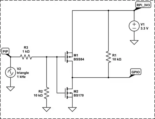
Figure 1 shows the voltage at the drain pin of an IRF530N NMOS for the circuit topology shown in fig. 2, but without resistor R2, and with M1's drain connected directly to a digital input pin on the microcontroller. (n.b. For this discussion, assume the microcontroller's input pin circuit does not provide voltage clamping protection diodes.)

The preshoot pulses observed at the corners of the voltage signal at M1's drain pin (fig. 1) occur because the MOSFET capacitively couples the edge of each state transition on the +12V side through its gate-drain capacitance to to drain pin on +5V logic side. The amplitude of these voltage spikes can be large enough to damage the circuitry of the microcontroller's digital input pin. For example, if a microcontroller's digital input pin has a minimum rated input voltage of -0.5 V, and a maximum rated voltage of 5.5 V, the signal shown in fig. 1 approaches the -0.5 V minimum, and it clearly exceeds the +5.5 V maximum.
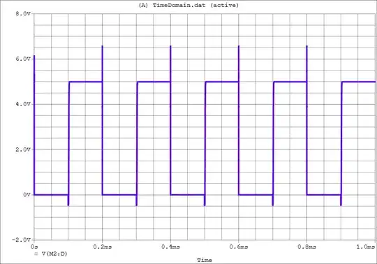
enter image description here

Figure 1.


There are various ways to manage this problem—e.g., see this EE.SE message thread: Schottky diodes or regular ones for input protection circuit.

Note that modern microcontrollers usually provide the two voltage clamping protection diodes shown in the linked page; they are part of the circuitry that implements a digital input pin. If this is the case, you provide resistor R2 connected in series between the MOSFET's drain pin and the microcontroller's digital input pin as shown in fig. 2.

schematic

simulate this circuit – Schematic created using CircuitLab

Figure 2.

If the addition of R2 does not reduce the amplitude of the preshoot voltage spikes to acceptable levels at the digital input pin, you can try adding a small value resistor in series with M1's gate, and adding a small capacitance (e.g., 2 nF) between M1's drain and ground. Note, however, that adding these components—and in particular, adding the capacitor—will slow down M1's switching times.

Jim Fischer
  • 3,074
  • 11
  • 15