I have master device / board that is connecting to PC USB. On board is LDO (1A) with 5V USB input and 1.8V - 3.6V output. LDO powers master board but also slave boards (different boards designed by others, not me) that can be connected / disconnected to / from master anytime (hot plugging). There is option that master device takes power from slave boards and in this case LDO is disabled.
Problem is current surge. When the master device is powered and there is communication with PC, if slave boards are connected, due to surge current (charging caps on slave boards) there is voltage drop on LDO and master is reseted with lost PC connection. To handle this I used few ohm resistor between master / target VCC line. But now I am looking for better solution.
There are 0603 and 0805 PTC fuses (for example to hold 250mA and trip 500mA, with 0.5-2.3 Ohm) that can be found on many USB boards, but reaction time is (I guess) a little slow (0.1 sec).
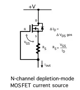
I found that depletion N-MOSFET can be used as current limiter...
but problem is that, when master board is powered by slave boards current will flow in opposite direction, over FET diode, and thre will be (at least) 0.7V voltage drop / difference that is unacceptable, because master / slave devices should work on same voltage.
There is low cost microchip (bidirectional) LND01.
I found hspice model online, but don't know about diode connection, and how to define this in transistor description inside hspice, to simulate something...
M1 Vd Vg Vs ? LND01 W=40m L=1.5u AD=1 AS=1 PD=4 PS=4
Don't know if some J-FET's and how (for example J105) can be used for this.
All integrated solution that I found online, are not bidirectional, or / and not working on low voltage (1.8V). All commercial products that I know for, use two regulators to handle this, one for master, and another for target, and if master is "powered" by target than there is voltage sensing with adjusting master device LDO output.
EDIT: I an new to J-FET's, but there is no internal diode and I guess that they are symmetrical devices, so they can work on the same way, with Vgs= 0 or Vgd=0. If I simulate J105 with Vgs=0, connect one side to 5V, and another to 100 uF capacitor in series with 5 ohm resistor current will draw and other side (capacitor voltage) will end at 5V. If I switch direction D-S, current in opposite direction, cap is again charged to 5V. I can't see white smoke in simulator, so don't know if I am doing something wrong. Can with JFET Vgs=0 current flow in the both ways?
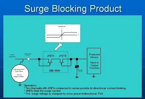
I found this...
Can't find DEI1600 datasheet, so don't know if this J-FET's are connected back to back like SIC J-FET's with internal diode, or not.

