4

What does the following symbol represent?

Mystery Symbol

Update 1: For some context:

enter image description here

ARF
  • 5,199
  • 9
  • 43
  • 71

2 Answers2

5

A MOSFET (p-channel).

The central pin is the Substrate or Bulk, the outwards arrow means that it's a p-MOS.

Courtesy of Wikipedia

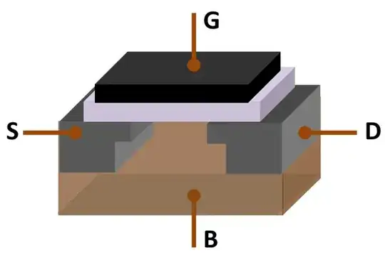
The image (found on Wiki) shows how the MOSFET is internally; the Bulk contact is connected to the substrate where the transistor is build upon. If not tied to the source, the Body effect changes the threshold voltage, altering the current output.

Usually Bulk and Source are connected together, like in the case of discrete MOSFETs; however, in integrated circuits design, like VLSI (very large scale integration), entire rows of transistors (all p or n channel) share the same substrate, and thus have it connected to Vdd.

clabacchio
  • 13,501
  • 4
  • 42
  • 80
  • All symbols for p-MOS I found have the bulk pin connected to the source pin. Example: https://upload.wikimedia.org/wikipedia/commons/thumb/1/1b/IGFET_P-Ch_Dep_Labelled.svg/150px-IGFET_P-Ch_Dep_Labelled.svg.png – ARF Mar 30 '12 at 11:48
  • 1
    @ArikRaffaelFunke because in packaging it's often (if not always) like this; in integrated circuits, however, it's not possible and bulk is always the same for all pMOS in a logic block. That leads to Early effect problems. Consider that MOS transistors are used at 99% in integrated circuits. – clabacchio Mar 30 '12 at 11:56
  • I am not sure I am following: in the schematic, the bulk, source and drain pins are connected to three different nodes. This symbol seems represent a 4-lead device which is actually used as a 4-lead device. – ARF Mar 30 '12 at 11:58
  • No, no no. Gate is the third pin, while bulk is the fourth, and not usually used in discrete components. Correction to previous comment: Body effect, not Early. – clabacchio Mar 30 '12 at 12:00
  • I think you misunderstood my last comment. I added the schematic to give you the context in which the symbol appears and see how the leads are connected. – ARF Mar 30 '12 at 12:05
  • @clabacchio - interestingly, Arik appears to be correct. If you look at the diagram they have separated source and substrate connections. and have connected a 1 M resistor between them. Very unusual. – Russell McMahon Mar 30 '12 at 12:07
  • @ArikRaffaelFunke Q2 is quite strangely connected; but in integrated circuits design, the Bulk contact is not always connected to the source, but always to Vcc in the case of pMOS, and for the transistors which don't have the source to Vdd (like pass-transistors) this leads to Body effect. That may be the case of Q1 – clabacchio Mar 30 '12 at 12:08
  • @RussellMcMahon true, Q2 is not clear to me; but Q1 is more normal, as I said to Arik – clabacchio Mar 30 '12 at 12:11
5

The other answers and comments about P Channel MOSFETS and substrate or bulk connection are essentially correct in a modern context but MAY be wrong here.

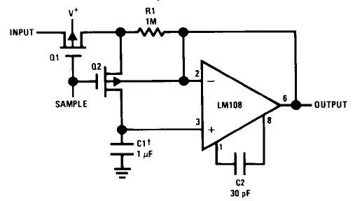
Tha symbol is from a 1989 circuit diagram in this data sheet and the component is connected and used in a different manner from anything that I am aware of that is available on the market now.

When an IC or MOSFET is made it is fabricated on a "substrate" or base layer. This is usually made of silicon. In special cases sapphire may be used - this has two very special main effects - more on that soon.

When the IC is formed a diode is created automatically between the drain and source (if a MOSFET is being made) via the substrate material. This diode is ALWAYS reverse biased in operation. The substrate layer is not made available externally as a separate connection.
SO the device shown also has a substrate connection BUT it is made available for separate connection as can be seen in he diagram - to connect 2 pins with a 1M resistor as they do means hey must be available externally.

When sapphire is used there is NO conductive substrate layer. This is also referred to as "silicon on insulator". The two main effects are reduced capacitance effects (no reverse biased diode junction acting as a varactor diode) and NO REVERSE DIODE.SOS is very expensive and so is very rare.

Russell McMahon
  • 150,303
  • 18
  • 213
  • 391
  • As you describe it, it seems an unusual use of the Bulk pin...are you aware of discrete Fetx with that pin available? – clabacchio Mar 30 '12 at 12:29
  • @clabacchio The ALD1106 is a pair of NFETs with a common bulk terminal. It is very uncommon because it is not used in 99.9999.....% of discrete circuits. – W5VO Mar 30 '12 at 13:18
  • @W5VO yeah, and IMHO it makes very little sense – clabacchio Mar 30 '12 at 13:24
  • @clabacchio - I have never seen such a discrete in 30 years in the industry, although I remember seeing circuits like this a lot in NSC databooks from the 1980s. N (or P) Channel ICs would normally have the substrate connected to the most negative (or positive) voltage in the circuit. I guess the schematic was drawn by an IC designer rather than an applications engineer :) – MikeJ-UK Mar 30 '12 at 13:28
  • @MikeJ-UK that's also what I knew (I'm not old enough for 80's stuff :D); but look at Q2: it seems explicitly connected to use the bulk in a different way (tied to the output), probably some black magic trick – clabacchio Mar 30 '12 at 13:38
  • @clabacchio - Yes, I was wondering the same. Possibly it's to minimize the leakage from C1 - but I'm not an IC design expert. – MikeJ-UK Mar 30 '12 at 13:46
  • 1
    Russell, talking about SOS processes, there are a lot of ways to skin that cat. These days, you can get SOI with a silicon wafer, and triple-well bulk CMOS processes. Neither are particularly expensive anymore. – W5VO Mar 30 '12 at 13:52