When using a BJT as switch, you do NOT usually imagine that \$\beta=60\$. You might in certain unusual circumstances. But usually not.
Let's take a look at the 2N3904 from OnSemi. The datasheet is found here: 2N3904 datasheet. That way we can share our views together.
Go look at Figure 16, Collector Saturation Region, in that datasheet. There you will see a nice chart. For operating a BJT as a switch, you want to have \$V_{CE}\$ be relatively low -- say under \$200\:\text{mV}\$ if possible. This \$200\:\text{mV}\$ itself varies from device to device, by the way. So what you want to do is to find that knee you can see in those curves there and move your eye a little to the right of the knee. In this case, they provide 4 curves -- one for each of some "practical" values for \$I_C\$. Let's say you feel that \$I_C=30\:\text{mA}\$ is closest to your needs (I hope it isn't a lot more than \$100\:\text{mA}\$!) Looking at that curve, you can see that about \$I_B = 1\:\text{mA}\$ is a "good" place. That's because the \$V_{CE_{sat}} \approx 200\:\text{mV}\$ there. (Large signal BJTs might show a higher value for a "good" \$V_{CE}\$ on their curves, so you have to adapt your mind to each device.)
So this gives you a figure of \$\beta = \frac{I_C}{I_B} \approx 30\$, here. Not 60! More, these are "typical" values. Not guaranteed ones. So a designer might look at this curve to get a "feel" for things, such as what to expect for \$V_{CE_{sat}}\$ for the transistor they are considering and also about what kind of \$\beta\$ would be reasonable. But then they would design in some serious margin. In this case, I'd say that you should plan on a \$\beta \approx 15\$. Now, a lot of designers just arbitrarily and without even checking a small signal BJT datasheet at all, just set \$\beta = 10\$ since they know it is being used as a switch. That's a pretty good bright line, if you are into bright lines. If you aren't and instead want to double check things, then go get the datasheet and look. Then make a reasoned judgment. Chances are, your saturation \$\beta\$ will be somewhere in the \$10 - 20\$ range. For large signal devices, you'd best check the datasheet.
Let's look at this another way. Look at Figure 17, now. The one called “ON” Voltages. Note here on the chart that they show some curves for \$\frac{I_C}{I_B} = 10\$? That is the datasheet writer providing information on the case where the BJT is "saturated" and operating as a switch. This is a very common use, so they provide standard curves. But notice that they selected \$\beta=10\$ for the purposes of charting some typical data (at some temperature.) This is yet another clue for you. It tells you that it isn't unreasonable to apply \$\beta=10\$ in this case. You should learn to read datasheets like this. It helps.
So now suppose you have this circuit:
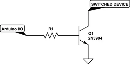
simulate this circuit – Schematic created using CircuitLab
You look at Figure 17 and see the \$V_{BE_{sat}}\$ curve shows about \$815\:\text{mV}\$ for \$I_C = 30\:\text{mA}\$. So that is your estimate now for \$V_{BE}\$ for purposes of your switch calculations. Let's be different and stick with my \$\beta_{sat}=15\$, too, as well as \$I_c=30\:\text{mA}\$ for now. We'll take your figure of \$V_{CC}=5\:\text{V}\$.
So now you compute:
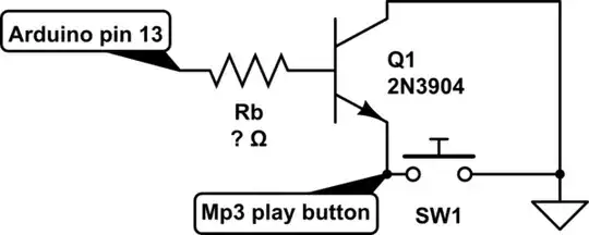
\$R_1 = \frac{Vcc-V_{BE_{sat}}}{I_B} = \frac{Vcc-V_{BE_{sat}}}{\frac{I_C}{\beta_{sat}}} = \beta_{sat}\cdot\frac{Vcc-V_{BE_{sat}}}{I_C}= 15\cdot\frac{5\:\text{V}-815\:\text{mV}}{30\:\text{mA}} = 2092.5\:\Omega\$
Round that up to \$2.2\:\text{k}\Omega\$ or down to \$1800\:\Omega\$. Both probably will work fine. Note that I took an exact \$V_{BE_{sat}}=815\:\text{mV}\$ from the chart? Actual parts will vary on that. So I might have, to be conservative, picked a value of \$V_{BE_{sat}}=1\:\text{V}\$ to be safer. That's partly why slight adjustments of the resistor value are probably okay. We are just approximating things, anyway.
Another note here is that the equation I used doesn't include any drop of voltage at the Arduino I/O pin. In fact, there will be a drop. So the output will not actually be \$5\:\text{V}\$. Especially not when supplying \$2\:\text{mA}\$ or so. The output of an Arduino actually has an equivalent resistor of about \$100\:\Omega\$ present. This is essentially just the ON resistance of the internal MOSFETs used by the Arduino CPU. But it does matter a little. In this case, you can expect a drop of about \$V_{drop}=100\:\Omega\cdot I_B = 200\:\text{mV}\$. As you can see, subtracting that means that we probably should have used \$4.8\:\text{V}\$ instead of \$5\:\text{V}\$ in our calculations. If you want to see the full equation with that included, then:
\$R_1 = \beta_{sat}\cdot\frac{Vcc-V_{BE_{sat}}}{I_C} - 100\:\Omega\$
In short, all you do is subtract off the expected impedance of the I/O pin. And as you can see, that's merely \$100\:\Omega\$ less that previously calculated.
Additional Note: But why \$V_{BE_{sat}}=1\:\text{V}\$ and not \$V_{BE_{sat}}=2\:\text{V}\$ to be even safer still? Well, it turns out that if we used an \$I_C\$ value that is 10 times higher, the needed \$V_{BE_{sat}}\$ would only be about \$60\:\text{mV}\$ more. So we only need to increase \$V_{BE_{sat}}\$ by one or two of these \$60\:\text{mV}\$ amounts in order to not only cover our bases, but cover them pretty well. So, really, \$V_{BE_{sat}}=1\:\text{V}\$ would be very conservative and there is no need to estimate any more than that here.
So I think by now you should realize just how many different "reasoned" elements are being brought into a calculation. This is why rounding to a nearest value usually works just fine for you. There are decisions that swing this way, and that way, but the main thing is that you get yourself into the ballpark without missing any important details. There are cases where precision counts. But this isn't one of them.
