3

No, I'm not asking you about my whole design - just one little bit of it.

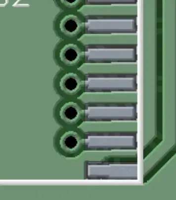
I have SMT devices, and I am currently pushing 8 pins on each side of some chips (SO24) straight through to the other side of the board with vias:

Vias close together

Having so many vias so close together - is it really a good idea?

Should I be staggering them more, or spacing them out a bit? Will this make the board too weak? The board itself is designed to be plugged in and out of breadboard many times, so may be stressed quite a bit.

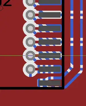
Btw - same area as it would look after fabrication:

PostFab

Majenko
  • 56,223
  • 9
  • 105
  • 189
  • Do you have a reason not to stagger them? – Kevin Vermeer Jul 19 '11 at 16:27
  • Laziness? ;) No, no reason, but I don't want to move them around if I don't need to. – Majenko Jul 19 '11 at 16:28
  • 1
    Looks like you have a ground pour, don't you want that ground pour to be able to separate the vias? – Kellenjb Jul 19 '11 at 16:30
  • @Kellenjb not necessarily. The ground pour is more out of habit - it's not actually required for this board. – Majenko Jul 19 '11 at 16:32
  • 1
    I am more interested in the physical integrity of the board than the electrical properties. Is putting vias this close together a Bad Idea™? – Majenko Jul 19 '11 at 16:33
  • BTW - it passes the DRC for my PCB fabricator's tolerances. – Majenko Jul 19 '11 at 16:42
  • This silk screen is too close to solder paste area. With silk printer being sloppy, the solder paste inspection will be difficult to tune. –  Jul 19 '11 at 19:29
  • @rocket My fabricator does a damn fine job - never had any screening problems before - they all seem accurate to within 0.000001 mil ;) – Majenko Jul 19 '11 at 19:48

2 Answers2

5

It won't harm the PCB at all. The material is so stiff that even a slot over the length of the vias won't weaken it noticeably.
The image may be a bit misleading too. The via holes are actually indicated by the smallest gray circles, the darker gray is the annular copper. So the distance between the vias is greater than the via's diameter.
I wouldn't worry about it.

stevenvh
  • 145,832
  • 21
  • 457
  • 668
1

The holes in a row will weaken the board a little bit, but probably not enough to be significant. Have you ever tried snapping 0.1" matrix protoboard by hand? It's quite resilient.

I do suggest you increase the copper clearance on the IC pads so that you don't get ground plane between them. That will make assembly easier. Unless you need the ground there for signal isolation reasons, so-called "guard ring".

markrages
  • 20,015
  • 7
  • 60
  • 97
  • Not sure if I can increase the clearance on the pads in this software - I could just not fill that area ;) – Majenko Jul 19 '11 at 16:34
  • looks like you are using "pcb". You can change clearance by selecting then doing a command like :changeclearsize(selectedpads, 30, mil) – markrages Jul 19 '11 at 16:37
  • 1
    Yup - if you can call it using... Fighting with is more accurate (although the newer versions have improved) – Majenko Jul 19 '11 at 16:38
  • I figured this was going to be a board with solder mask. – Kellenjb Jul 19 '11 at 16:43
  • @kellenjb that it is. – Majenko Jul 19 '11 at 17:09
  • I have seen problems with this kind of ground finger, even with solder mask. It was under a 1208 capacitor. In about one percent of the production units, the mask would not quite cover the edge of the ground copper, and a bridge would form. Adjusting the solder mask bloat would probably cure this, but if the copper doesn't need to be there anyway, why borrow trouble? – markrages Jul 19 '11 at 20:49
  • +1 I agree that the PCB will be plenty strong enough even with those holes drilled in it. In general I prefer to stagger holes far enough apart so the ground plane can squeeze through them rather than creating a slot in the ground plane, for EMI/EMC reasons.( a, b c ). It looks like letting that ground plane squeeze through does not matter in this case. – davidcary Jun 22 '13 at 21:14