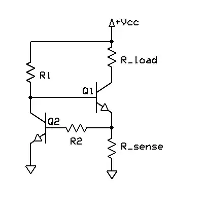
Another alternative to dealing with the voltage dropped over Rsense (which in your transistor feedback circuit must be ~0.6-0.7V to operate) you should investigate using an Op-amp. You can drop 10 times less voltage over Rsense for the designed current limit, by reducing the size of Rsense by 10, and having an op-amp in non-inverting configuration with a gain of 10 to amplify the voltage built up over Rsense while current flows through it.
Here is how it might look:
simulate this circuit – Schematic created using CircuitLab
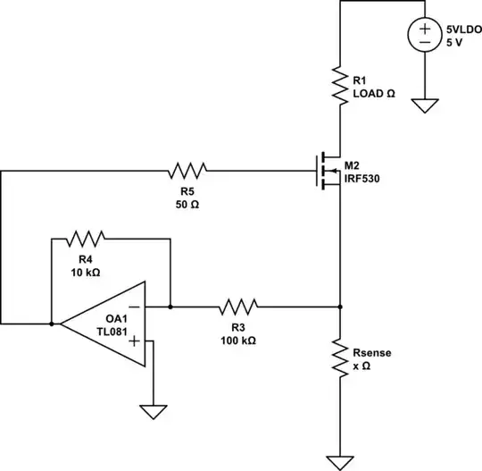
M2 being Q1 in your design, as a low-side current limiting FET using Rsense and it's voltage as the current limiting control signal. The Opamp will sense this value, amplify it by 10 with the shown resistors, and then control the FET as if it was a linear resistor. The issue with this is, your load (shown by R1) may not want a floating ground like this, so you have to be careful.
EDIT: I have fixed the circuit to use negative feedback, so as the voltage over Rsense increases, the output of the op-amp decreases, thus turning off the N channel FET. The FET will be in the linear resistance region so it may get hot while current-limiting. The gate of the FET needs to be above 0V, at least above Vgs(min) to begin conducting. At initial condition, the op-amp should have the FET full on, at 5V(or whatever you power the op-amp with). Once M2 conducts Rsense will begin to build up voltage as the current flows, and the gate voltage will decrease in response. The idea is that the analog feedback reaches an equilibrium state, providing a constant current on the output by dynamically driving the MOSFET gate up/down in response to the load.
The important part here is by using some basic analog feedback to get the same result as if Rsense was large, and controlled a (MOSFET or BJT) transistor's base, using the op-amp in a fairly trivial use-case allows you to have a very small value resistance as a current shunt resistor.
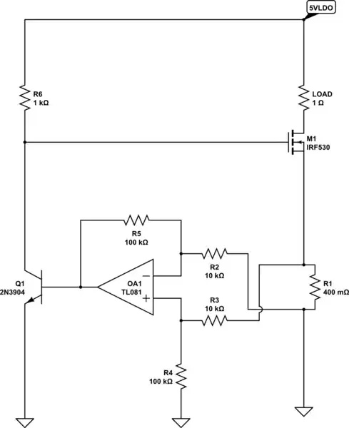
simulate this circuit
EDIT: The above schematic retains the standard way of the voltage over Rsense controlling the base of an NPN transistor, but has an intermediate difference amplifier with a gain of 10 to make only 60-70mV turn on the NPN base rather than needing 600-700mV.
Be aware that if you want a high-side current limit load switch, you will need to use a P channel FET, and they have (a little) more complex control circuits.
