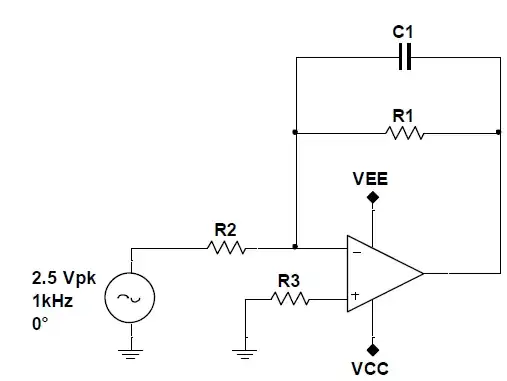
I have seen this type of circuit design a few times, but am not sure why it is needed. Considering the schematic below, what is the purpose of resistor R3?
I have seen this type of circuit design a few times, but am not sure why it is needed. Considering the schematic below, what is the purpose of resistor R3?
It depends on the opamp. In the old days when we had to trudge to school barefoot in the snow uphill both ways, opamps inputs drew enough current to matter to many circuits. For such opamps, the imbalance in current between the two inputs, called the input offset current was lower than the total current drawn by each input. You could cancel out the common current drawn by both inputs by driving them with the same impedance, leaving the additional voltage offset due to the lower offset current. In your example, R3 is there to present the same impedance to the + input as is driving the - input, which is R1//R2.
Generally, this is the case with opamps that have bipolar transistors on the input, such as the common jellybean LM324.
Today a lot of ompamps have MOS inputs, so the input bias current is so low as to not matter in most cases. Since the current is due to leakage and not biasing the internal transistors, you can't really count on its direction. There generally is no bias current offset spec. In this case, there is no point in trying to match the impedance driving each input. You do sometimes see this on MOS-input opamps due to a religious conviction or someone applying a rule of thumb without thinking about what it's for and when it's valid.
It it to mitigate the input leakage current of the OPAMP
The OPAMP will attempt to keep the difference between + & - to equal zero. The input leakage current of the OPAMP in conjunction with gain resistors will produce a voltage at the - pin. If the + pin was tied to 0V there would now be an offset error voltage
By providing a resistance to 0V (usually the parallel equivalent resistance of R1 & R2) the offset error due to this leakage current can be mitigated.
Here is a good writeup on the affect. http://www.analog.com/static/imported-files/tutorials/MT-038.pdf
R1 is there to counter-act any small DC offset since the integral of any DC offset tends to infinity. These offsets can come from source errors (your source may not be exactly a sign wave) or they can be intrinsic to the Op-Amp (known as input offset voltage).
edit: oh wait, you're asking about R1, not R3. Incidentally, it amused me when someone up-voted my initial wrong answer.
R3 is there to counteract the effect of input bias current (basically the assumption that an op-amp has no current flowing into its input terminals isn't true, so you need to account for it).