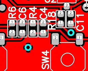
My EDA software (PCAD, but I guess others do this too) adds thermal reliefs on vias in a copper pour. What's the use? Vias aren't soldered. (I know why you use them on regular PTH pads)

My EDA software (PCAD, but I guess others do this too) adds thermal reliefs on vias in a copper pour. What's the use? Vias aren't soldered. (I know why you use them on regular PTH pads)

What the other guys have said is very true. I'll add that about 10 or 15 years ago I stopped using thermal reliefs. Since that time, maybe 30-50K PCB's have been manufactured and I've never had a problem.
In a production environment soldering to pins/pads/vias/holes directly connected to large planes isn't really an issue due to the temperature profile of the ovens, and that the ovens tend to heat the whole board and not just the pads that are being soldered.
When hand soldering on a PCB without thermal reliefs there can be an issue, as the others have pointed out, but in my opinion the advantages of no thermal reliefs are far greater than easier hand soldering.
Here's some of the advantages of no thermal reliefs:
So, in the end, I don't use thermal reliefs and I've had zero problems (other than the occasional hand-solder issue which is easy to overcome).
IPC2221 Section 9.1.3 says:
9.1.3 Thermal Relief in Conductor Planes Thermal relief is only required for holes that are subject to soldering in large conductor areas (ground planes, voltage planes, thermal planes, etc.). Relief is required to reduce soldering dwell time by providing thermal resistance during the soldering process
I think most of times is not necessary to thermally relive a via.
To ensure that the copper pour doesn't conduct the heat away when the board is soldered, which will result in bad solder joints. Vias are sometimes filled with solder, to increase reliability.
Thermal reliefs are optional with the software I use; you can probably make them ordinary vias, if you wish. Tent them, if you don't want them soldered.
A proper thermal relief on TH connections is a must for Lead free wave soldering. It is impossible to get 50% solder fill (or 47mil, which ever is less) on ground connections without thermal relief, especially on +90mil thick PCBs. There is IPC 2221A section 9.1.3, which has very good recommendation. I have seen best results on two 10mil web spoke designs for +3 ground plane PCBs.