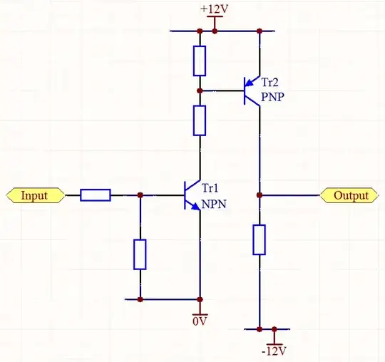
My attempt at a solution.
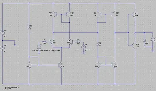
R5 and R6 are only there to model source resistance and are not part of the circuit. C1 and R4 are used as load for simulation.
V4: input source (10MHz 0.5 duty ratio 0-to-5V square wave for simulation)
V3: reference source (2.5V for simulation)
V1: +12V supply
V2: -12V supply
It's basically an op amp or comparator. I only did some transient simulations to check it out. It might suit your needs. Main drawbacks are complexity, 1:1 output level sensitivity to the supply levels, no output short circuit protection.
You would need to trim up the supplies a little bit if you need to get closer to +/-12V output. I would recommend increasing R1 and R3 to 5k or 10k or 20k. This would lower quiescent power consumption but would decrease output current capability--but you probably would not need to drive a lot of current with this, right? You would want to play with the values to get it right for your needs.
V3 sets the switching threshold. There is no hysteresis. You might be able to set up a positive feedback loop from output to input to make schmitt trigger to add hysteresis.
The output stage could probably also be changed to push-pull common emitter amplifiers instead of followers to get a wider output swing.
Schematic:
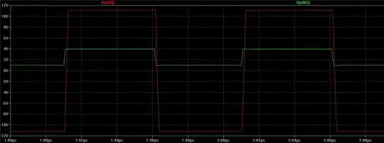
Simulation: