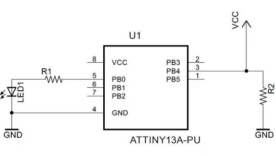
7

MCU: ATTiny13

I noticed this after trying to debug why pushing my switch (connected via R2, a 507kOhm pulldown resistor) makes the LED dimmer while depressed. The switch was powered by the same supply line as the Vcc input to the microcontroller.

Upon disconnecting the Vcc input (Pin 8), I noticed that the LED was still lit when the switch was depressed. If I removed a connection from the ground pin 4, the LED still lit up, but less brighter.

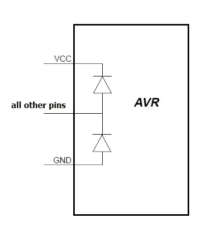
The circuit below represents what I observed. The switch is removed to simplify the problem:

enter image description here

Why does this happen, and how can I stop it? It is interfering with the output when the button is depressed.

Here is a picture of the circuit on a breadboard. The supply line (5V is the red wire, Ground is black):

enter image description here

tgun926
  • 2,766
  • 12
  • 37
  • 59
  • 1
    Sounds like a construction problem. By that schematic, there is no way the LED could light up with Vcc disconencted. Of course, without the micro's Vcc pin connected, a whole lot of nothing is going to happen. – Matt Young Aug 01 '14 at 14:17
  • 1
    Can you show the switch in your circuit? – Scott Seidman Aug 01 '14 at 14:19
  • 1
    @ScottSeidman the switch is connected between Vcc and the node to pin 3 and R2, however this occurs without a physical switch. – tgun926 Aug 01 '14 at 14:24
  • 1
    @MattYoung - no, that is not the case. This circuit is outside the allowed usage, but probably will work. It seems like the previous circuit was simplified, removing the switch, to understand this particular puzzling-if-not-seen-before (but well known) behavior. – Chris Stratton Aug 01 '14 at 14:26
  • 4
    Surely that isn't the whole circuit. Almost certainly one of the I/O pins is being held at Vdd or is being pulled up to Vdd. – Olin Lathrop Aug 01 '14 at 14:32
  • 1
    @ChrisStratton I was under the impression that Vcc was totally disconnected. If only the Vcc pin is disconnected, then yes, the clamping diodes make sense. – Matt Young Aug 01 '14 at 14:33
  • 1
    @OlinLathrop No, this is what is on the breadboard. R2 is 680kOhm. – tgun926 Aug 01 '14 at 14:44
  • 2
    Connecting an I/O pin to a higher voltage than VCC leads to undefined behavior in case of many microcontrollers. The microcontroller is in an undefined state and anything can happen. – vsz Aug 01 '14 at 15:21
  • 2
    No, that clearly can't be what you actually hooked up. If it were connected according to your description, there would be no source of power at all, and therefore no way for the LED to light. Perhaps the bottom of R2 is actually connected to Vdd? – Olin Lathrop Aug 01 '14 at 17:02
  • @OlinLathrop I have added a picture of the circuit. Black is 0V, red is Vcc (5V) – tgun926 Aug 01 '14 at 22:25
  • 1
    And just like we knew would be the case, one of the microcontroller pins is tied to Vdd. – Olin Lathrop Aug 01 '14 at 22:53
  • @OlinLathrop I'm not seeing a difference between the schematic and the breadboard - could you explain? – tgun926 Aug 01 '14 at 23:08
  • 1
    You need to refine both your text and your diagram. While you provide some clues in the comments they are oncomplete. reader should be able to look at the diagram and see what you are doing and read the text and understand the various conditions that apply. | You say "Vcc is not connected" - which is a completely ambiguous statement. Vcc can mean a pin of that name or a voltage - and in this case it means BOTH. "Vcc_supply" is not connected to Vcc_processor_pin BUT is connected to "some other processor pin which it has no valid reason to be connected to". ... – Russell McMahon Aug 02 '14 at 10:55
  • 1
    ... If you are doing dangerously randomly random things, at a minimum you should clearly describe the randomly random things you are doing - and why you think that this randomness makes any sense. eg WHY connect Vcc_supply to PB4? Why do you think doing this makes any sense at all? Why are you in any way surprised that the result is rubbish? What were you were trying to do by doing this? Why not do it in some legal and non-random way? – Russell McMahon Aug 02 '14 at 10:56
  • @RussellMcMahon Does the question make sense now without having to decipher the comments? – tgun926 Aug 02 '14 at 13:34
  • 1
    We can see that pin 3 is connected to Vdd, despite your assertion that it is not. As everyone has been trying to tell you, that partially powers up the microcontroller thru the high side protection diode on pin 3. What the micro does in that situation is undefined, so it should be no surprise that enough current makes it out of pin 5 to visibly light the LED. I really don't see the mystery here. It's what everyone has been saying right from the start. – Olin Lathrop Aug 02 '14 at 14:00

5 Answers5

23

Inputs of many modern CMOS devices have ESD protection diodes from the I/O pins to the supply rails, which hope to divert transient overvoltages to the supply before they cause damage.

A side effect of this is that the chip can, at least to a degree be powered through an I/O pin, once the pin rises enough against the (unsupplied) supply to forward bias the diode. Even in technologies without explicit protection diodes, it could happen to a degree, though often resulted in very unreliable operation (classic mistake - forget to power a chip and see it "sort of" work - I did it myself with an SPI flash this past January that somehow never got a ground, and would provide expected responses right up until I tried to write flash locations).

Generally you do not want to power a chip this way - it is outside the absolute maximum ratings, and the protection diode may not be sized to carry the full operating current. You do see it at times though, both in intentional experiments, such as an RF-powered ATTiny RFID tag emulator experiment, or accidentally in cases such as trying to measure power consumption of a sleeping MCU and having it actually draw power from your serial debug port rather than the supply you are trying to measure.

Chris Stratton
  • 33,491
  • 3
  • 44
  • 90
  • 1
    Thanks, makes sense to me. Is this the same reason the LED becomes dimmer when I make the input pin's voltage high? Do I just have to use a series resistor to lower the input voltage to fix this? – tgun926 Aug 01 '14 at 14:27
  • 1
    That could not be answered without seeing the schematic and the program code. Sounds like its own question. – Chris Stratton Aug 01 '14 at 14:30
  • 1
    Good answer. I've done this with Microchip processors as well. Bugger of time figuring it out the first time. – Adam Head Aug 01 '14 at 15:51
8

The datasheet for your device has this table:

enter image description here

In this table, VCC means the voltage applied to the VCC pin, not the net in your circuit which you have labelled VCC.

Since you have not applied any voltage to the VCC pin, you must not apply more than 0.5V to any other pin. Your PB4 connection is violating this rule.

Ben Voigt
  • 2,865
  • 1
  • 23
  • 34
4

Current flows thru internal clamping diodes.

Internal circuitry (simplified) looks like this:

enter image description here

In this Atmel document (random application note containing information about clamping diodes) you can read:

To protect the device from voltages above VCC and below GND, the AVR has internal clamping diodes on the I/O pins (see Figure 1). The diodes are connected from the pins to VCC and GND and keep all input signals within the AVR’s operating voltage (see Figure 2). Any voltage higher than VCC + 0.5V will be forced down to VCC + 0.5V (0.5V is the voltage drop over the diode) and any voltage below GND - 0.5V will be forced up to GND - 0.5V.

Kamil
  • 6,004
  • 9
  • 43
  • 60
1

Just a addendum to Chris Strattons correct answer.

You are indeed powering the device through the protection diodes. There are several ways of providing ESD protection and all of them involve using diodes on the pins to connect to a rail inside. So your conduction path and internal power of your chip will be at least 1 diode drop below the supplied "power" on the pin.

You can test this out by measuring the the Vcc pin it will be about 0.7V lower than Vcc.

When you disconnect the ground, you are pulling less current through the protection diodes and shifting the operating point of the voltage supplied to the LED. But by a little bit, so this may not account for the difference.

The protection diodes are designed to handle Amps of current during a ESD strike so they are fine with this little trickle.

Your danger in operating the chip this way is that you could induce latch up, but most chips are designed to be able to NOT latch up in these conditions so that isn't a concern so much. But a possibility.

Another danger will depend upon what the exact nature of the ESD protection on chip. If it is a clamping style and you have a high dV/dT event then the clamp might fire and short out the supply. But this is also unlikely.

placeholder
  • 30,170
  • 10
  • 63
  • 110
  • 4
    "The protection diodes are designed to handle Amps of current during a ESD strike so they are fine with this little trickle." This is a fallacious viewpoint. An ESD strike is a transient, that consists of quite a small charge, so low energy dissipation, even if the instantaneous voltage and current are large. Running current continuously through these diodes will cause heat problems that don't occur during the ESD transient. – Ben Voigt Aug 01 '14 at 15:48
  • 3
    "The protection diodes are designed to handle Amps of current during a ESD strike so they are fine with this little trickle." not sure I agree. I've seen data sheets (Xilinx spartan FPGAs for example) which allow you to use the protection diodes with a series resistor for level-shifting, but specify a fairly low maximum current, which you must use to size the resistor. IIRC the limit would be around just lighting a single LED, though that was a finer-grained technology, so it might be higher for this part, if Atmel chose to characterize it. – Chris Stratton Aug 01 '14 at 15:50
  • 1
    What you don't know is that I've designed these I/O cells myself which are part of some standard libraries and I was Mentored by a person whose ESD designs/IP is in Most modern IC. You just need to look at SEM's of parts that final during a ESD strike to realize how silly it to say that currents during an event are low or that he high current are meaningless. Most of the metal in an ESD structure is there to reduce resistance to the conduction. Current is current and the voltage excursion cannot be exceeded during an event ergo, low low resistance. – placeholder Aug 01 '14 at 15:54
  • 2
    The apparent conclusion that this implies you can safely power the chip does not follow. Why, for example, does Xilinx tell you the limit for current through Spartan 3 protection diodes which they do allow you to forward bias is a mere 10 mA? http://www.xilinx.com/support/answers/19146.htm – Chris Stratton Aug 01 '14 at 17:56
  • 2
    @placeholder: Who said that "currents during an event are low"? Low resistance in this scenario actually makes heating during continuous flow worse, since the power dissipation is $V^2/R$. This in contrast to an ESD event where the charge transferred is pretty much fixed and the resistance doesn't affect the total energy dissipation. What the low resistance does provide is that very little of the charge will choose any other path. But that low resistance in the path doesn't mean there is good thermal dissipation... – Ben Voigt Aug 01 '14 at 17:57
  • @BenVoigt All voltages must be kept on chip to low values other wise you'll pop the gate oxide or potentially trigger a latchup (which is possible with the very high currents). This all means v. low resistance. Interestingly, the limit is on the contact structure not the Si (wrt current flow). To high HBM (and not a great spec either) the structure has to handle 1.3 A and that means an array of 80 X 80 contacts into the ESD diodes. THAT is not a small structure. Your argument for V^2/R doesn't hold. – placeholder Aug 01 '14 at 18:28
  • @ChrisStratton I don't recommend it, in fact that is in there. Also I reference your write up which says you shouldn't. wrt Xilinx, Don't confuse specs that are there to prevent latchup (Vdd driven at low impedance) to a scenario that is possible with the Vdd pins not connected. – placeholder Aug 01 '14 at 18:31
  • 2
    @placeholder: All your HBM analysis makes assumptions that are inapplicable to continuous currents. For ESD, the energy is $$q \Delta V$$. For this question, it is $$\int \frac{V^2}{R} dt$$ – Ben Voigt Aug 01 '14 at 18:35
  • @BenVoigt a structure that handles large amperage will continue to do so. – placeholder Aug 01 '14 at 18:38
  • 2
    @placeholder: But that isn't designed to handle a large mean current, only a momentary pulse. There is a huge difference between a pulse and a continuous current with respect to thermal load. – Ben Voigt Aug 01 '14 at 18:49
  • @BenVoigt I wish I had a little more time so we could go onto chat. These are huge structures and voltages have to be limited, to emphasize, the contact structure needs to be made up of 6400 diodes in parallel (each capable of mA's) in one example of a shipping product. You can't pump high current at low voltages unless you light it up with a spark, any thing less than that isn't going heat it up. – placeholder Aug 01 '14 at 19:05
  • Some devices are constructed in such fashion that driving multiple milliamps into VDD through the protection diodes will work fine without adverse side-effects. Not all devices are so designed, however. I remember one CMOS logic chip I used which seemed to implement the protection for each pair of inputs using a bit of P-type material for each input and a bit of N-type material between them. The effect of this was that feeding 1mA into a pin driven above rail while the other pin was low would cause the circuit to behave like a PNP transistor between the input pins. – supercat Aug 01 '14 at 19:12
  • @supercat that is called a lateral PNP structure in CMOS and is sometimes used (even though it is a parasitic structure) with a Hfe barely above 1. – placeholder Aug 01 '14 at 19:29
  • 2
    @placeholder: Indeed; my point was that the protection structures are designed to protect the chip, and may do in ways one might not expect, and which may be detrimental to some applications. – supercat Aug 01 '14 at 20:17
0

You are probably powering the device through its protection diodes BUT the important thing is that you are doing something which is "illegal" and completely outside specification and anything can happen and you should not be surprised if it does.

Your circuit diagram is WRONG.
This is the REAL circuit diagram that you are using:

enter image description here

This is a hardware version of "garbage in, garbage out".

If you do something random and get a random result you should be happy - the universe is working as you'd expect.

More later maybe ...

Ricardo
  • 6,164
  • 20
  • 53
  • 89
Russell McMahon
  • 150,303
  • 18
  • 213
  • 391