6

I'm having difficulty working out required values of resistors \$R_C\$ and \$R_E\$ in the circuit below. Can't seem to find any formulas on the web.

schematic1![][1]

I know how to find \$R_1\$ and \$R_2\$:

$$R_1 = (\frac{R_2}{V_B} \times V_{CC})-R_2$$

$$R_2 = \frac{β_{DC} \times R_E}{10}$$

I'd appreciate any help you can give with this as I can't move forward with other calculations until I find values for \$R_C\$ and \$R_E\$.

Technical specs of circuit:

  • BJT BC108
  • Voltage divider bias used
  • \$I_{C(sat)} = 20mA\$
  • \$V_{CC} = 10V\$
  • 10μF coupling capacitors for the input and output connections
  • 100μF capacitor for the bypass capacitor
  • \$β_{DC} ≈ 200\$
  • Voltage gain without bypass capacitor = 1.5

I plotted a DC Load Line and the Q-point is at \$I_C = 10mA\$ and \$V_{CE} = 5V\$.

DC Load Line Schematic

somers
  • 161
  • 2
  • 4
  • 12

3 Answers3

7

Warning - rules of thumb being used!!

I always try and get about 0.5 to 1V on the emitter (lets say 0.75V). This means the base will be at about 1.45V and this allows you to calculate R1 and R2 (but be prepared to revise those values should the base current drawn be a little high).

You want 10mA thru the collector and this is virtually the same current through the emitter so now you can decide what Re is - 0.75V/10mA = 75 ohms.

At 10mA collector current you want collector to be half rail so that means Rc is 5V/10mA = 500 ohm. Another rule of thumb - current thru R1 and R2 should be about one-tenth of Hfe lower than Ic. If Hfe is 200 then current in R1 and R2 is about 10mA/20 = 0.5mA.

R1 + R2 therefore should equal 10V/0.5mA = 20 kohm.

R2 needs to be smaller than R1 to develop about 1.45V on the base and on a 10V supply I can immediately see that R2 being about 2k9 would take 0.5mA to develop 1.45V. This leaves R1 as 17k1 ohms.

I'd use 3k0 for R2 and an 18k for R1 for practical reasons of obtainability.

C3 depends on your lowest frequency input and how much voltage gain you need. Without C3 there is a voltage gain of approximately Rc / Re = 6.667. If you want more gain use C3 but be prepared to put a small resistor in series with it to linearize the gain over the full desired bandwidth.

Andy aka
  • 456,226
  • 28
  • 367
  • 807
  • Adding one point: The presence of C3 suggests either the intent is to get maximum gain for the range of frequencies of interest, and possibly to introduce a low-cut filter effect. Amplification factor in the freq range of interest will then depend entirely on transistor beta, which can be quite variable, and also not linear over a large swing of output voltage (and Ic). To reduce that variability and non-linearity (at a cost of reducing the amplification) an additional resistor is interposed at the emitter (Re in Andy's answer). – gwideman Apr 05 '14 at 00:02
5

You have 4 resistors and thus, 4 degrees of freedom. You need four independent and consistent design constraints to find a unique set of four resistor values.

Some of the possible design constraints are:

(1) input impedance

(2) output impedance

(3) AC gain

(4) DC collector current

The input impedance is approximately

$$Z_{in} = R_1||R_2||r_{\pi} $$

The output impedance is approximately

$$Z_{out} = R_C||r_o $$

The AC gain is approximately

$$A_v = -g_mR_C||r_o $$

The DC collector current is approximately

$$I_C = \frac{V_{BB} - V_{BE}}{\frac{R_{BB}}{\beta} + \frac{R_E}{\alpha}} $$

where

$$V_{BB} = V_{CC}\frac{R_2}{R_1 + R_2} $$

$$R_{BB} = R_1||R_2 $$

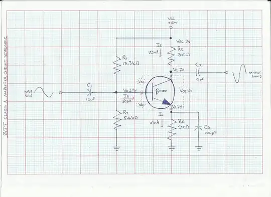
Since the only constraints you've specified are \$I_C\$ and \$V_{CE}\$, you must use some engineering judgement ('best guess', 'rules of thumb') to justify your choice of resistor values as, e.g, Andy aka has demonstrated.

As another example of how to proceed, let's first calculate the small signal parameters:

$$g_m = \frac{I_C}{V_T} = \frac{10mA}{25mV} = 0.4S$$

$$r_{\pi} = \frac{\beta}{g_m} = \frac{200}{0.4S} = 500 \Omega$$

$$r_o = \frac{V_A}{I_C} = \frac{80V}{10mA} = 8k\Omega$$

Now, it is clear that the input impedance must be less than \$r_{\pi}=500\Omega\$ which is quite low.

Assume that the desired (magnitude) voltage gain is \$|A_v| = 100\$, then

$$R_C \approx \frac{|A_v|}{g_m}=\frac{100}{0.4S} = 250\Omega $$

Since \$R_C<<r_o\$, we can ignore \$r_o\$ from here.

The DC collector voltage will be

$$V_C = V_{CC} - I_C R_C = 10V - 10mA \cdot 250\Omega = 7.5V$$

You've specified that \$V_{CE} = 5V\$ so the DC emitter voltage is

$$V_E = V_C - V_{CE} = 7.5V - 5V = 2.5V$$

Thus, the required value for \$R_E\$ is

$$R_E = \frac{V_E}{I_E} \approx \frac{V_E}{I_C} = \frac{2.5V}{10mA} = 250\Omega$$

Assuming \$V_{BE} = 0.7V\$, the voltage across \$R_2\$ is

$$V_{R2} = V_E + V_{BE} = 2.5V + 0.7V = 3.2V$$

Now, a rule of thumb for operating point stability is to set the current through \$R_2\$ to be 10 times the DC base current

$$I_{R2} = 10\cdot I_B = 10 \cdot \frac{I_C}{\beta} = \frac{10}{200}10mA = 500\mu A $$

Thus, the required value of \$R_2\$ is

$$R_2 = \frac{V_{R2}}{I_{R2}} = \frac{3.2V}{500\mu A} = 6.4k\Omega$$

By KCL, the current through \$R_1\$ is

$$I_{R1} = (10 + 1)I_B = 11 \cdot 50\mu A = 550 \mu A $$

The voltage across \$R_1\$ is

$$V_{R1} = V_{CC} - V_{R2}= 10V - 3.2V = 6.8V $$

Thus, the required value for \$R_1\$ is

$$R_1 = \frac{V_{R1}}{I_{R1}} = \frac{6.8V}{550\mu A} = 12.4k\Omega$$

Using E96 (1%) values for the resistors yields

$$R_1 = 12.4k\Omega $$

$$R_2 = 6.34k\Omega $$

$$R_E = 249\Omega$$

$$R_C = 249\Omega$$

Alfred Centauri
  • 26,630
  • 1
  • 25
  • 63
  • (and Andy aka), thanks a lot for the help. I'm new at this and am trying to absorb what you've both said. I will get back to you. – somers Apr 04 '14 at 22:36
  • Output impedance is a pretty common constraint as Alfred has pointed out and it's worth saying that the output impedance of the circuit is basically Rc. This is because the collector is akin to a constant current generator and has typically several tens of kohm compliance. Several tens of kohm in parallel with an Rc of several hundred ohms doesn't alter the dominant impedance being largely Rc. – Andy aka Apr 05 '14 at 09:22
  • @Alfred Centauri, thank you very much for your time I'm reading through your latest post. There was a constraint which I forgot to include which is that the voltage gain without a bypass capacitor is 1.5. Can I simply substitute that value in place of the 100 in your example? – somers Apr 05 '14 at 22:27
  • @stevesy, no you can't for the reason that the gain formula is valid only when the emitter is at AC ground, i.e., $R_E$ is bypassed with a capacitor that is an AC short circuit at the operating frequencies. The gain without the $C_3$ is approximately $ -\frac{R_C}{R_E} $ if $R_E$ is 'large enough'. With this additional constraint, $R_C = 1.5 \cdot R_E$, added to the constraint $V_{CE} = 5V$, $R_C$ and thus, the AC (bypassed) gain is fixed: $R_C = 300 \Omega \rightarrow A_v = -120$ – Alfred Centauri Apr 05 '14 at 22:51
  • By which I mean would an re value need to be included for av? – somers Apr 05 '14 at 23:02
  • @stevesy, if by $A_v$ you mean the AC gain (the gain assuming $C_3$ is an AC short circuit), then no. If by $A_v$ you mean the gain without $C_3$ then yes as my previous comment details. – Alfred Centauri Apr 05 '14 at 23:30
  • @Alfred Centauri, I meant the AC gain without C3. I got an re value of 2.5Ω by dividing 25mV by 10mA. I'm sorry, I don't understand how you got the 300Ω and -120 and I'm unsure of what way to calculate all of this with/without the bypass capacitor. – somers Apr 05 '14 at 23:58
  • @Alfred Centauri, The specs say that a bypass capacitor should be used yet they give a formula for voltage gain without a bypass capacitor. This is adding to my confusion. – somers Apr 06 '14 at 00:06
  • @Alfred Centauri, just to mention, as regards finding RC and RE I had thought about using the voltage gain formula Av = RC/RE or Av = RC/re + RE, pick 2 resistor values so that their ratio gave 1.5. If the latter formula were used, subtract the value obtained for re from RE to get its value. Would that work? – somers Apr 06 '14 at 01:14
  • @stevesy, to expand on what I earlier wrote, if $R_E$ is 'large enough', $r_e$ is insignificant in the gain calculation. Since, in this case, $r_e \approx 2.5\Omega$ and $R_E = 200 \Omega$, including $r_e$ in the gain calculation doesn't significantly change the result. As to how I calculated $R_C$, we have that $R_C = 1.5 \cdot R_E$ and $V_{CE} = 5V$, thus we must have $V_{CC} - V_{CE} = I_C(R_C + R_E) = I_C(R_C + \frac{R_C}{1.5}) $ which gives $R_C = 300 \Omega$ and $R_E = 200\Omega$ – Alfred Centauri Apr 06 '14 at 01:55
  • @Alfred Centauri, thank you sir. Would I be correct in saying that, with the bypass filter included, Av would be 300Ω/2.5Ω = 120? – somers Apr 06 '14 at 09:53
  • @stevesy, I assume you're aware that $g_m = \frac{\alpha}{r_e}$ and, as I wrote in my answer, the gain, with the emitter resistor bypassed is $-g_mR_C$ (ignoring $r_o$) thus, we can also write the gain as $-\alpha\frac{R_C}{r_e} \approx -\frac{R_C}{r_e} = -\frac{300}{2.5}$ – Alfred Centauri Apr 06 '14 at 11:24
  • @Alfred Centauri, I've uploaded the schematic I've drawn up. Can you let me know what you think, thanks. – somers Apr 06 '14 at 22:54
  • @Alfred Centauri, I think VE should be 2.2V but calculations say it's 2V. – somers Apr 06 '14 at 23:03
  • @stevesy, what is your reasoning for $V_E = 2.2V$? – Alfred Centauri Apr 06 '14 at 23:46
  • @Alfred Centauri, VC was 7V i.e. 10V-(10mA*300Ω). VE=VC-VCE = 7-5=2V – somers Apr 07 '14 at 02:46
  • @stevesy, that's correct reasoning leading to $V_E = 2V$. There's also $V_E = 10mA \cdot 200\Omega = 2V$ so why do you think it should otherwise? – Alfred Centauri Apr 07 '14 at 02:51
  • @Alfred Centauri, because the Base Voltage VB came to 2.9V (5.4kΩ/13.3kΩ + 5.4kΩ)*10 = 2.9V – somers Apr 07 '14 at 10:33
  • @Alfred Centauri, subtracting the voltage across the Emitter Base Junction VBE from VB gives VE = 2.9 - 0.7 = 2.2V – somers Apr 07 '14 at 10:40
  • @stevesy, 2.9V is the open circuit base voltage $V_{BB}$ - the base voltage when there is zero base current. Since there is base current the voltage is less than 2.9V. The correct formula for the DC base voltage is $V_B = V_{BB} - I_B\cdot R_{BB} = 2.9V - 50\mu A \cdot 5.4k||13.3k = 2.7V$ – Alfred Centauri Apr 07 '14 at 12:19
  • @Alfred Centauri, thanks so much for your help : ] – somers Apr 07 '14 at 13:07
0

there is difference between voltage and power amplifiers in class A:

the distinction of between voltage and power amplifier is somewhat artificial since useful power (product of voltage and current) is always developed in the load resistance through which current flows.the difference between the two types is really one of degree.it is a question of how much voltage and how much power.a voltage amplifier is designed to achieve maximum voltage amplification.it is however no important to rise the power level.on the other hand a power amplifier is designed to obtain maximum output power.

voltage amplifier: the transistor with high beta is used in the circuit.(beta > 100) the input resistance of the transistor is sought to be quite low as compared to the collector load Rc. a relatively high load Rc is used in the collector.voltage amplifier are always operated at low collector current.(Rc=4 to 10k) output impedance:(high ~12kΩ)

power amplifier: the size of power transistor is made considerably larger in order to dissipate the heat during operation. the transistor with low beta is used in the circuit.(beta=5 to 20) output impedance:(low ~200Ω)

musefian
  • 149
  • 2
  • 12