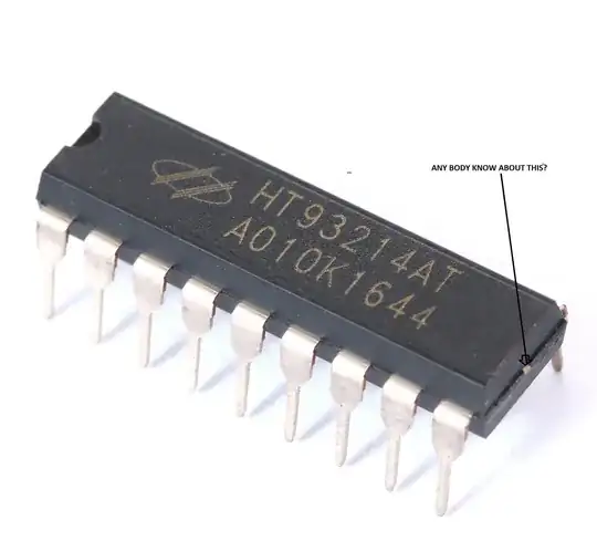
I have seen an unusual mark on an IC. Can anyone tell me does it have any functional or testing significance?
I have seen an unusual mark on an IC. Can anyone tell me does it have any functional or testing significance?
Perhaps this image would help.
As you can see the metal pressing to connect the pins to the chip have a central bar that is exposed at the end of the resin.
Plastic IC packages such as that one are made by transfer molding resin around a metal leadframe (with the IC die and bonding wires already mounted).
The molding process looks like this schematic animation.
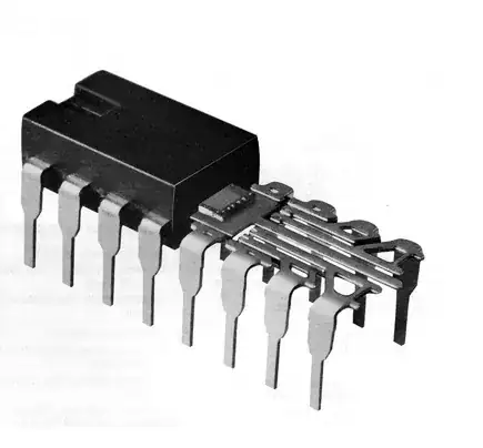
The leadframes look like this before the dies are attached.

And like this after the dies are attached and the transfer molding process is complete.
Following the molding process, a metal stamping die is used to shear off the unwanted support bits of the leadframe (and to form the leads into the desired shape from the flat). The bits hanging out the ends are support for the die attach platform. The support bits attached to the ends of the leads are sheared off and discarded.

In the above photo, note the epoxy filling the gaps between the legs. That's 'flash' on the mold, and gets sheared off when the leads are formed. If you could closely at the OP's photo, you can see where the bits were broken off (on the sides, between the legs).